D a t a S he et , R e v . 1 . 3 , J a n . 2 00 6
Q u a d L I U TM
Q u a d E 1 / T 1 / J 1 L i ne I n t e r f a c e C o m p o n e nt f o r
L o n g - a n d S h o r t - H a ul A p pl i c a t i o n s
P E F 22 5 0 4 E , P E F 2 2 5 04 H T , V e r s i o n 2 . 1
C o m m u ni c a t i o n s
�Edition 2006-01-25
Published by Infineon Technologies AG,
81726 München, Germany
© Infineon Technologies AG 2006.
All Rights Reserved.
Attention please!
The information herein is given to describe certain components and shall not be considered as a guarantee of
characteristics.
Terms of delivery and rights to technical change reserved.
We hereby disclaim any and all warranties, including but not limited to warranties of non-infringement, regarding
circuits, descriptions and charts stated herein.
Information
For further information on technology, delivery terms and conditions and prices please contact your nearest
Infineon Technologies Office (www.infineon.com).
Warnings
Due to technical requirements components may contain dangerous substances. For information on the types in
question please contact your nearest Infineon Technologies Office.
Infineon Technologies Components may only be used in life-support devices or systems with the express written
approval of Infineon Technologies, if a failure of such components can reasonably be expected to cause the failure
of that life-support device or system, or to affect the safety or effectiveness of that device or system. Life support
devices or systems are intended to be implanted in the human body, or to support and/or maintain and sustain
and/or protect human life. If they fail, it is reasonable to assume that the health of the user or other persons may
be endangered.
�QuadLIUTM
PEF 22504
PEF 22504 E, Quad E1/T1/J1 Line Interface Component for Long- and Short-Haul Applications
Revision History: 2006-01-25, Rev. 1.3
Previous Version: Preliminary Data Sheet 2005-11-07
Chapter, Table
Chapter 2.3,
Chapter 5
Subjects (major changes since last revision)
The QuadLIUTM is now available in PG-TQFP-144-17 package also
Trademarks
ABM®, ACE®, AOP®, ARCOFI®, ASM®, ASP®, DigiTape®, DuSLIC®, EPIC®, ELIC®, FALC®, GEMINAX®, IDEC®,
INCA®, IOM®, IPAT®-2, ISAC®, ITAC®, IWE®, IWORX®, MUSAC®, MuSLIC®, OCTAT®, OptiPort®, POTSWIRE®,
QUAT®, QuadFALC®, SCOUT®, SICAT®, SICOFI®, SIDEC®, SLICOFI®, SMINT®, SOCRATES®, VINETIC®,
10BaseV®, 10BaseVX® are registered trademarks of Infineon Technologies AG. 10BaseS™, EasyPort™,
VDSLite™ are trademarks of Infineon Technologies AG. Microsoft® is a registered trademark of Microsoft
Corporation, Linux® of Linus Torvalds, Visio® of Visio Corporation, and FrameMaker® of Adobe Systems
Incorporated.
Data Sheet
3
Rev. 1.3, 2006-01-25
�QuadLIUTM
PEF 22504
Table of Contents
Preface . . . . . . . . . . . . . . . . . . . . . . . . . . . . . . . . . . . . . . . . . . . . . . . . . . . . . . . . . . . . . . . . . . . . . . . . 11
1
1.1
1.2
1.3
Introduction . . . . . . . . . . . . . . . . . . . . . . . . . . . . . . . . . . . . . . . . . . . . . . . . . . . . . . . . . . . . . . . . . . . .
Features . . . . . . . . . . . . . . . . . . . . . . . . . . . . . . . . . . . . . . . . . . . . . . . . . . . . . . . . . . . . . . . . . . . . . . .
Logic Symbol . . . . . . . . . . . . . . . . . . . . . . . . . . . . . . . . . . . . . . . . . . . . . . . . . . . . . . . . . . . . . . . . . . .
Typical Applications . . . . . . . . . . . . . . . . . . . . . . . . . . . . . . . . . . . . . . . . . . . . . . . . . . . . . . . . . . . . . .
12
13
15
16
2
2.1
2.2
2.3
2.4
2.5
Pin Descriptions . . . . . . . . . . . . . . . . . . . . . . . . . . . . . . . . . . . . . . . . . . . . . . . . . . . . . . . . . . . . . . . .
Ball Diagram P/PG-LBGA-160-1 (top view) . . . . . . . . . . . . . . . . . . . . . . . . . . . . . . . . . . . . . . . . . . . .
Ball Diagram P/PG-LBGA-160-1 (bottom view) . . . . . . . . . . . . . . . . . . . . . . . . . . . . . . . . . . . . . . . . .
Pin Diagram P-TQFP-144 . . . . . . . . . . . . . . . . . . . . . . . . . . . . . . . . . . . . . . . . . . . . . . . . . . . . . . . . . .
Pin Definitions and Functions . . . . . . . . . . . . . . . . . . . . . . . . . . . . . . . . . . . . . . . . . . . . . . . . . . . . . . .
Pin Strapping . . . . . . . . . . . . . . . . . . . . . . . . . . . . . . . . . . . . . . . . . . . . . . . . . . . . . . . . . . . . . . . . . . .
17
17
17
19
20
64
3
3.1
3.2
3.3
3.4
3.5
3.5.1
3.5.1.1
3.5.2
3.5.2.1
3.5.2.2
3.5.3
3.5.4
3.5.5
3.5.5.1
3.6
3.6.1
3.7
3.7.1
3.7.2
3.7.3
3.7.3.1
3.7.3.2
3.7.3.3
3.7.3.4
3.7.3.5
3.7.4
3.7.5
3.7.6
3.7.7
3.7.8
3.7.8.1
3.7.8.2
3.7.8.3
3.7.8.4
3.7.9
3.8
3.8.1
3.8.2
3.8.3
3.8.4
Functional Description . . . . . . . . . . . . . . . . . . . . . . . . . . . . . . . . . . . . . . . . . . . . . . . . . . . . . . . . . . . 65
Hardware . . . . . . . . . . . . . . . . . . . . . . . . . . . . . . . . . . . . . . . . . . . . . . . . . . . . . . . . . . . . . . . . . . . . . . 65
Software . . . . . . . . . . . . . . . . . . . . . . . . . . . . . . . . . . . . . . . . . . . . . . . . . . . . . . . . . . . . . . . . . . . . . . . 66
Functional Overview . . . . . . . . . . . . . . . . . . . . . . . . . . . . . . . . . . . . . . . . . . . . . . . . . . . . . . . . . . . . . . 66
Block Diagram . . . . . . . . . . . . . . . . . . . . . . . . . . . . . . . . . . . . . . . . . . . . . . . . . . . . . . . . . . . . . . . . . . 67
Functional Blocks . . . . . . . . . . . . . . . . . . . . . . . . . . . . . . . . . . . . . . . . . . . . . . . . . . . . . . . . . . . . . . . . 67
Asynchronous Micro Controller Interface (Intel or Motorola mode) . . . . . . . . . . . . . . . . . . . . . . . . . 67
Mixed Byte/Word Access . . . . . . . . . . . . . . . . . . . . . . . . . . . . . . . . . . . . . . . . . . . . . . . . . . . . . . . 68
Serial Micro Controller Interfaces . . . . . . . . . . . . . . . . . . . . . . . . . . . . . . . . . . . . . . . . . . . . . . . . . . 69
SCI Interface . . . . . . . . . . . . . . . . . . . . . . . . . . . . . . . . . . . . . . . . . . . . . . . . . . . . . . . . . . . . . . . . 69
SPI Interface . . . . . . . . . . . . . . . . . . . . . . . . . . . . . . . . . . . . . . . . . . . . . . . . . . . . . . . . . . . . . . . . 73
Interrupt Interface . . . . . . . . . . . . . . . . . . . . . . . . . . . . . . . . . . . . . . . . . . . . . . . . . . . . . . . . . . . . . . 74
Boundary Scan Interface . . . . . . . . . . . . . . . . . . . . . . . . . . . . . . . . . . . . . . . . . . . . . . . . . . . . . . . . . 76
Master Clocking Unit . . . . . . . . . . . . . . . . . . . . . . . . . . . . . . . . . . . . . . . . . . . . . . . . . . . . . . . . . . . . 78
PLL (Reset and Configuring) . . . . . . . . . . . . . . . . . . . . . . . . . . . . . . . . . . . . . . . . . . . . . . . . . . . . 79
Line Coding and Framer Interface Modes . . . . . . . . . . . . . . . . . . . . . . . . . . . . . . . . . . . . . . . . . . . . . 80
Bipolar Violation Detection . . . . . . . . . . . . . . . . . . . . . . . . . . . . . . . . . . . . . . . . . . . . . . . . . . . . . . . . 81
Receive Path . . . . . . . . . . . . . . . . . . . . . . . . . . . . . . . . . . . . . . . . . . . . . . . . . . . . . . . . . . . . . . . . . . . 83
Receive Line Interface . . . . . . . . . . . . . . . . . . . . . . . . . . . . . . . . . . . . . . . . . . . . . . . . . . . . . . . . . . . 84
Receive Line Coding . . . . . . . . . . . . . . . . . . . . . . . . . . . . . . . . . . . . . . . . . . . . . . . . . . . . . . . . . . . . 84
Receive Line Interface . . . . . . . . . . . . . . . . . . . . . . . . . . . . . . . . . . . . . . . . . . . . . . . . . . . . . . . . . . . 84
“Generic” Receiver Interface . . . . . . . . . . . . . . . . . . . . . . . . . . . . . . . . . . . . . . . . . . . . . . . . . . . . 85
Receive Line Monitoring Mode (RLM) . . . . . . . . . . . . . . . . . . . . . . . . . . . . . . . . . . . . . . . . . . . . . 86
Monitoring Application using RLM . . . . . . . . . . . . . . . . . . . . . . . . . . . . . . . . . . . . . . . . . . . . . . . . 86
Redundancy Application using RLM . . . . . . . . . . . . . . . . . . . . . . . . . . . . . . . . . . . . . . . . . . . . . . 87
General Redundancy Applications . . . . . . . . . . . . . . . . . . . . . . . . . . . . . . . . . . . . . . . . . . . . . . . 89
Loss-of-Signal Detection . . . . . . . . . . . . . . . . . . . . . . . . . . . . . . . . . . . . . . . . . . . . . . . . . . . . . . . . . 91
Receive Equalization Network . . . . . . . . . . . . . . . . . . . . . . . . . . . . . . . . . . . . . . . . . . . . . . . . . . . . . 92
Receive Line Attenuation Indication . . . . . . . . . . . . . . . . . . . . . . . . . . . . . . . . . . . . . . . . . . . . . . . . 92
Receive Clock and Data Recovery . . . . . . . . . . . . . . . . . . . . . . . . . . . . . . . . . . . . . . . . . . . . . . . . . 92
Receive Jitter Attenuator . . . . . . . . . . . . . . . . . . . . . . . . . . . . . . . . . . . . . . . . . . . . . . . . . . . . . . . . . 92
Receive Jitter Attenuation Performance . . . . . . . . . . . . . . . . . . . . . . . . . . . . . . . . . . . . . . . . . . . 95
Jitter Tolerance (E1) . . . . . . . . . . . . . . . . . . . . . . . . . . . . . . . . . . . . . . . . . . . . . . . . . . . . . . . . . . 96
Output Jitter . . . . . . . . . . . . . . . . . . . . . . . . . . . . . . . . . . . . . . . . . . . . . . . . . . . . . . . . . . . . . . . . . 98
Output Wander . . . . . . . . . . . . . . . . . . . . . . . . . . . . . . . . . . . . . . . . . . . . . . . . . . . . . . . . . . . . . . 98
Dual Receive Elastic Buffer . . . . . . . . . . . . . . . . . . . . . . . . . . . . . . . . . . . . . . . . . . . . . . . . . . . . . . . 99
Additional Receiver Functions . . . . . . . . . . . . . . . . . . . . . . . . . . . . . . . . . . . . . . . . . . . . . . . . . . . . . 100
Error Monitoring and Alarm Handling . . . . . . . . . . . . . . . . . . . . . . . . . . . . . . . . . . . . . . . . . . . . . . 100
Automatic Modes . . . . . . . . . . . . . . . . . . . . . . . . . . . . . . . . . . . . . . . . . . . . . . . . . . . . . . . . . . . . . . 101
Error Counter . . . . . . . . . . . . . . . . . . . . . . . . . . . . . . . . . . . . . . . . . . . . . . . . . . . . . . . . . . . . . . . . . 101
One-Second Timer . . . . . . . . . . . . . . . . . . . . . . . . . . . . . . . . . . . . . . . . . . . . . . . . . . . . . . . . . . . . 101
Data Sheet
4
Rev. 1.3, 2006-01-25
�QuadLIUTM
PEF 22504
Table of Contents
3.9
3.9.1
3.9.2
3.9.3
3.9.4
3.9.5
3.9.6
3.9.6.1
3.9.6.2
3.9.7
3.10
3.11
3.11.1
3.11.2
3.11.3
3.11.4
3.11.5
3.11.6
3.12
Transmit Path . . . . . . . . . . . . . . . . . . . . . . . . . . . . . . . . . . . . . . . . . . . . . . . . . . . . . . . . . . . . . . . . . .
Transmit Line Interface . . . . . . . . . . . . . . . . . . . . . . . . . . . . . . . . . . . . . . . . . . . . . . . . . . . . . . . . .
Transmit Clock TCLK . . . . . . . . . . . . . . . . . . . . . . . . . . . . . . . . . . . . . . . . . . . . . . . . . . . . . . . . . . .
Automatic Transmit Clock Switching . . . . . . . . . . . . . . . . . . . . . . . . . . . . . . . . . . . . . . . . . . . . . . .
Transmit Jitter Attenuator . . . . . . . . . . . . . . . . . . . . . . . . . . . . . . . . . . . . . . . . . . . . . . . . . . . . . . .
Dual Transmit Elastic Buffer . . . . . . . . . . . . . . . . . . . . . . . . . . . . . . . . . . . . . . . . . . . . . . . . . . . . .
Programmable Pulse Shaper and Line Build-Out . . . . . . . . . . . . . . . . . . . . . . . . . . . . . . . . . . . . .
QuadFALCTM V2.1 Compatible Programming with XPM(2:0) Registers . . . . . . . . . . . . . . . . . .
Programming with TXP(16:1) Registers . . . . . . . . . . . . . . . . . . . . . . . . . . . . . . . . . . . . . . . . . .
Transmit Line Monitor . . . . . . . . . . . . . . . . . . . . . . . . . . . . . . . . . . . . . . . . . . . . . . . . . . . . . . . . . .
Framer Interface . . . . . . . . . . . . . . . . . . . . . . . . . . . . . . . . . . . . . . . . . . . . . . . . . . . . . . . . . . . . . . . .
Test Functions . . . . . . . . . . . . . . . . . . . . . . . . . . . . . . . . . . . . . . . . . . . . . . . . . . . . . . . . . . . . . . . . .
Pseudo-Random Binary Sequence Generation and Monitor . . . . . . . . . . . . . . . . . . . . . . . . . . . . .
In-Band Loop Generation, Detection and Loop Switching . . . . . . . . . . . . . . . . . . . . . . . . . . . . . . .
Remote Loop . . . . . . . . . . . . . . . . . . . . . . . . . . . . . . . . . . . . . . . . . . . . . . . . . . . . . . . . . . . . . . . . .
Local Loop . . . . . . . . . . . . . . . . . . . . . . . . . . . . . . . . . . . . . . . . . . . . . . . . . . . . . . . . . . . . . . . . . . .
Payload Loop-Back . . . . . . . . . . . . . . . . . . . . . . . . . . . . . . . . . . . . . . . . . . . . . . . . . . . . . . . . . . . .
Alarm Simulation . . . . . . . . . . . . . . . . . . . . . . . . . . . . . . . . . . . . . . . . . . . . . . . . . . . . . . . . . . . . . .
Multi Function Ports . . . . . . . . . . . . . . . . . . . . . . . . . . . . . . . . . . . . . . . . . . . . . . . . . . . . . . . . . . . . .
102
102
103
103
104
105
105
106
107
108
109
110
110
111
112
113
113
114
114
4
4.1
4.1.1
4.2
4.2.1
Register Description . . . . . . . . . . . . . . . . . . . . . . . . . . . . . . . . . . . . . . . . . . . . . . . . . . . . . . . . . . . .
Detailed Control Register Description . . . . . . . . . . . . . . . . . . . . . . . . . . . . . . . . . . . . . . . . . . . . . . . .
Control Registers . . . . . . . . . . . . . . . . . . . . . . . . . . . . . . . . . . . . . . . . . . . . . . . . . . . . . . . . . . . . . .
Detailed Status Register Description . . . . . . . . . . . . . . . . . . . . . . . . . . . . . . . . . . . . . . . . . . . . . . . .
Status Registers . . . . . . . . . . . . . . . . . . . . . . . . . . . . . . . . . . . . . . . . . . . . . . . . . . . . . . . . . . . . . .
116
116
120
191
194
5
Package Outlines . . . . . . . . . . . . . . . . . . . . . . . . . . . . . . . . . . . . . . . . . . . . . . . . . . . . . . . . . . . . . . 220
6
6.1
6.1.1
6.1.2
6.1.3
6.1.4
6.1.4.1
6.1.4.2
6.1.4.3
6.1.4.4
6.1.5
6.1.6
6.1.6.1
6.1.6.2
6.2
6.3
6.4
6.4.1
6.4.2
Electrical Characteristics . . . . . . . . . . . . . . . . . . . . . . . . . . . . . . . . . . . . . . . . . . . . . . . . . . . . . . . .
AC Characteristics . . . . . . . . . . . . . . . . . . . . . . . . . . . . . . . . . . . . . . . . . . . . . . . . . . . . . . . . . . . . . .
Master Clock Timing . . . . . . . . . . . . . . . . . . . . . . . . . . . . . . . . . . . . . . . . . . . . . . . . . . . . . . . . . . .
JTAG Boundary Scan Interface . . . . . . . . . . . . . . . . . . . . . . . . . . . . . . . . . . . . . . . . . . . . . . . . . . .
Reset . . . . . . . . . . . . . . . . . . . . . . . . . . . . . . . . . . . . . . . . . . . . . . . . . . . . . . . . . . . . . . . . . . . . . . .
Asynchronous Microprocessor Interface . . . . . . . . . . . . . . . . . . . . . . . . . . . . . . . . . . . . . . . . . . . .
Intel Bus Interface Mode . . . . . . . . . . . . . . . . . . . . . . . . . . . . . . . . . . . . . . . . . . . . . . . . . . . . . .
Motorola Bus Interface Mode . . . . . . . . . . . . . . . . . . . . . . . . . . . . . . . . . . . . . . . . . . . . . . . . . . .
SCI Interface . . . . . . . . . . . . . . . . . . . . . . . . . . . . . . . . . . . . . . . . . . . . . . . . . . . . . . . . . . . . . . .
SPI Interface . . . . . . . . . . . . . . . . . . . . . . . . . . . . . . . . . . . . . . . . . . . . . . . . . . . . . . . . . . . . . . .
Digital Interface (Framer Interface) . . . . . . . . . . . . . . . . . . . . . . . . . . . . . . . . . . . . . . . . . . . . . . . .
Pulse Templates - Transmitter . . . . . . . . . . . . . . . . . . . . . . . . . . . . . . . . . . . . . . . . . . . . . . . . . . . .
Pulse Template E1 . . . . . . . . . . . . . . . . . . . . . . . . . . . . . . . . . . . . . . . . . . . . . . . . . . . . . . . . . .
Pulse Template T1 . . . . . . . . . . . . . . . . . . . . . . . . . . . . . . . . . . . . . . . . . . . . . . . . . . . . . . . . . . .
Capacitances . . . . . . . . . . . . . . . . . . . . . . . . . . . . . . . . . . . . . . . . . . . . . . . . . . . . . . . . . . . . . . . . . .
Package Characteristics . . . . . . . . . . . . . . . . . . . . . . . . . . . . . . . . . . . . . . . . . . . . . . . . . . . . . . . . . .
Test Configuration . . . . . . . . . . . . . . . . . . . . . . . . . . . . . . . . . . . . . . . . . . . . . . . . . . . . . . . . . . . . . .
AC Tests . . . . . . . . . . . . . . . . . . . . . . . . . . . . . . . . . . . . . . . . . . . . . . . . . . . . . . . . . . . . . . . . . . . .
Power Supply Test . . . . . . . . . . . . . . . . . . . . . . . . . . . . . . . . . . . . . . . . . . . . . . . . . . . . . . . . . . . . .
222
226
226
226
227
228
228
230
232
233
233
236
236
237
239
239
240
240
240
7
7.1
7.2
7.3
7.4
7.5
7.6
Operational Description . . . . . . . . . . . . . . . . . . . . . . . . . . . . . . . . . . . . . . . . . . . . . . . . . . . . . . . . .
Operational Overview . . . . . . . . . . . . . . . . . . . . . . . . . . . . . . . . . . . . . . . . . . . . . . . . . . . . . . . . . . . .
Device Reset . . . . . . . . . . . . . . . . . . . . . . . . . . . . . . . . . . . . . . . . . . . . . . . . . . . . . . . . . . . . . . . . . .
Device Initialization . . . . . . . . . . . . . . . . . . . . . . . . . . . . . . . . . . . . . . . . . . . . . . . . . . . . . . . . . . . . . .
Device Configuration in E1 Mode . . . . . . . . . . . . . . . . . . . . . . . . . . . . . . . . . . . . . . . . . . . . . . . . . . .
Device Configuration in T1/J1 Mode . . . . . . . . . . . . . . . . . . . . . . . . . . . . . . . . . . . . . . . . . . . . . . . . .
Device Configuration for Digital Clock Interface Mode (DCIM) . . . . . . . . . . . . . . . . . . . . . . . . . . . . .
243
243
243
244
244
245
248
Data Sheet
5
Rev. 1.3, 2006-01-25
�QuadLIUTM
PEF 22504
Table of Contents
8
8.1
8.2
8.3
Appendix . . . . . . . . . . . . . . . . . . . . . . . . . . . . . . . . . . . . . . . . . . . . . . . . . . . . . . . . . . . . . . . . . . . . .
Protection Circuitry . . . . . . . . . . . . . . . . . . . . . . . . . . . . . . . . . . . . . . . . . . . . . . . . . . . . . . . . . . . . . .
Application Notes . . . . . . . . . . . . . . . . . . . . . . . . . . . . . . . . . . . . . . . . . . . . . . . . . . . . . . . . . . . . . . .
Software Support . . . . . . . . . . . . . . . . . . . . . . . . . . . . . . . . . . . . . . . . . . . . . . . . . . . . . . . . . . . . . . .
249
249
249
249
Terminology . . . . . . . . . . . . . . . . . . . . . . . . . . . . . . . . . . . . . . . . . . . . . . . . . . . . . . . . . . . . . . . . . . 252
Data Sheet
6
Rev. 1.3, 2006-01-25
�QuadLIUTM
PEF 22504
List of Figures
Figure 1
Figure 2
Figure 3
Figure 4
Figure 5
Figure 6
Figure 7
Figure 8
Figure 9
Figure 10
Figure 11
Figure 12
Figure 13
Figure 14
Figure 15
Figure 16
Figure 17
Figure 18
Figure 19
Figure 20
Figure 21
Figure 22
Figure 23
Figure 24
Figure 25
Figure 26
Figure 27
Figure 28
Figure 29
Figure 30
Figure 31
Figure 32
Figure 33
Figure 34
Figure 35
Figure 36
Figure 37
Figure 38
Figure 39
Figure 40
Figure 41
Figure 42
Figure 43
Figure 44
Figure 45
Figure 46
Figure 47
Figure 48
Figure 49
Figure 50
Figure 51
Figure 52
Data Sheet
Logic Symbol . . . . . . . . . . . . . . . . . . . . . . . . . . . . . . . . . . . . . . . . . . . . . . . . . . . . . . . . . . . . . . . . . 15
Typical Multiple Link Application. . . . . . . . . . . . . . . . . . . . . . . . . . . . . . . . . . . . . . . . . . . . . . . . . . . 16
Typical Multiple Repeater Application between line #1 and Line #2. . . . . . . . . . . . . . . . . . . . . . . . 16
Top View of the Pin Configuration (Ball Layout) P/PG-LBGA-160-1 . . . . . . . . . . . . . . . . . . . . . . . 17
Bottom View of the Pin Configuration (Ball Layout) P/PG-LBGA-160-1 . . . . . . . . . . . . . . . . . . . . . 18
Pin Configuration P-TQFP-144-8 . . . . . . . . . . . . . . . . . . . . . . . . . . . . . . . . . . . . . . . . . . . . . . . . . . 19
Single Voltage Supply. . . . . . . . . . . . . . . . . . . . . . . . . . . . . . . . . . . . . . . . . . . . . . . . . . . . . . . . . . . 65
Dual Voltage Supply . . . . . . . . . . . . . . . . . . . . . . . . . . . . . . . . . . . . . . . . . . . . . . . . . . . . . . . . . . . . 66
Block Diagram . . . . . . . . . . . . . . . . . . . . . . . . . . . . . . . . . . . . . . . . . . . . . . . . . . . . . . . . . . . . . . . . 67
SCI Interface Application with Point To Point Connections . . . . . . . . . . . . . . . . . . . . . . . . . . . . . . 70
SCI Interface Application with Multipoint To Multipoint Connection . . . . . . . . . . . . . . . . . . . . . . . . 70
SCI Message Structure of QuadLIUTM . . . . . . . . . . . . . . . . . . . . . . . . . . . . . . . . . . . . . . . . . . . . . . 71
Frame Structure of QuadLIUTM SCI Messages . . . . . . . . . . . . . . . . . . . . . . . . . . . . . . . . . . . . . . . 72
Principle of Building Addresses and RSTA bytes in the SCI ACK Message of the QuadLIUTM . . . 72
Read Status Byte (RSTA) byte of the SCI Acknowledge (ACK). . . . . . . . . . . . . . . . . . . . . . . . . . . 73
SPI Read Operation . . . . . . . . . . . . . . . . . . . . . . . . . . . . . . . . . . . . . . . . . . . . . . . . . . . . . . . . . . . . 74
SPI Write Operation . . . . . . . . . . . . . . . . . . . . . . . . . . . . . . . . . . . . . . . . . . . . . . . . . . . . . . . . . . . . 74
Interrupt Status Registers . . . . . . . . . . . . . . . . . . . . . . . . . . . . . . . . . . . . . . . . . . . . . . . . . . . . . . . . 75
Block Diagram of Test Access Port and Boundary Scan . . . . . . . . . . . . . . . . . . . . . . . . . . . . . . . . 77
Flexible Master Clock Unit . . . . . . . . . . . . . . . . . . . . . . . . . . . . . . . . . . . . . . . . . . . . . . . . . . . . . . . 79
Behaviour of Bipolar Violation Detection . . . . . . . . . . . . . . . . . . . . . . . . . . . . . . . . . . . . . . . . . . . . 82
Receive System of one Channel . . . . . . . . . . . . . . . . . . . . . . . . . . . . . . . . . . . . . . . . . . . . . . . . . . 83
Recovered and Receive Clock Selection . . . . . . . . . . . . . . . . . . . . . . . . . . . . . . . . . . . . . . . . . . . . 84
General Receiver Configuration with Integrated Resistor and Analog Switches for Receive
Impedance Matching . . . . . . . . . . . . . . . . . . . . . . . . . . . . . . . . . . . . . . . . . . . . . . . . . . . . . . . . . . . 85
Principle of Receive Line Monitoring RLM (shown for one line) . . . . . . . . . . . . . . . . . . . . . . . . . . . 86
Monitoring Application using RLM (shown for one line) . . . . . . . . . . . . . . . . . . . . . . . . . . . . . . . . . 87
Redundancy Application using RLM (shown for one line) . . . . . . . . . . . . . . . . . . . . . . . . . . . . . . . 89
General Redundancy Application (shown for one line). . . . . . . . . . . . . . . . . . . . . . . . . . . . . . . . . . 90
Principle of Configuring the DCO-R and DCO-X Corner Frequencies . . . . . . . . . . . . . . . . . . . . . . 94
Jitter Attenuation Performance (E1) . . . . . . . . . . . . . . . . . . . . . . . . . . . . . . . . . . . . . . . . . . . . . . . . 96
Jitter Attenuation Performance (T1/J1). . . . . . . . . . . . . . . . . . . . . . . . . . . . . . . . . . . . . . . . . . . . . . 96
Jitter Tolerance (E1) . . . . . . . . . . . . . . . . . . . . . . . . . . . . . . . . . . . . . . . . . . . . . . . . . . . . . . . . . . . . 97
Jitter Tolerance (T1/J1). . . . . . . . . . . . . . . . . . . . . . . . . . . . . . . . . . . . . . . . . . . . . . . . . . . . . . . . . . 97
Output Wander . . . . . . . . . . . . . . . . . . . . . . . . . . . . . . . . . . . . . . . . . . . . . . . . . . . . . . . . . . . . . . . . 98
The Receive Elastic Buffer as Circularly Organized Memory . . . . . . . . . . . . . . . . . . . . . . . . . . . . 100
Transmit System of one Channel . . . . . . . . . . . . . . . . . . . . . . . . . . . . . . . . . . . . . . . . . . . . . . . . . 102
Transmit Line Interface . . . . . . . . . . . . . . . . . . . . . . . . . . . . . . . . . . . . . . . . . . . . . . . . . . . . . . . . . 103
Clocking and Data in Remote Loop Configuration . . . . . . . . . . . . . . . . . . . . . . . . . . . . . . . . . . . . 105
Measurement Configuration for E1 Transmit Pulse Template . . . . . . . . . . . . . . . . . . . . . . . . . . . 106
Measurement Configuration for T1/J1 Transmit Pulse Template . . . . . . . . . . . . . . . . . . . . . . . . . 106
Transmit Line Monitor Configuration. . . . . . . . . . . . . . . . . . . . . . . . . . . . . . . . . . . . . . . . . . . . . . . 108
Framer Interface (shown for one channel) . . . . . . . . . . . . . . . . . . . . . . . . . . . . . . . . . . . . . . . . . . 109
Remote Loop . . . . . . . . . . . . . . . . . . . . . . . . . . . . . . . . . . . . . . . . . . . . . . . . . . . . . . . . . . . . . . . . 112
Local Loop . . . . . . . . . . . . . . . . . . . . . . . . . . . . . . . . . . . . . . . . . . . . . . . . . . . . . . . . . . . . . . . . . . 113
Payload Loop . . . . . . . . . . . . . . . . . . . . . . . . . . . . . . . . . . . . . . . . . . . . . . . . . . . . . . . . . . . . . . . . 114
P/PG-LBGA-160-1 (Plastic Green Low Profile Ball Grid Array Package). . . . . . . . . . . . . . . . . . . 220
PG-TQFP-144-17 (Plastic Thin Quad Flat Package) . . . . . . . . . . . . . . . . . . . . . . . . . . . . . . . . . . 221
MCLK Timing . . . . . . . . . . . . . . . . . . . . . . . . . . . . . . . . . . . . . . . . . . . . . . . . . . . . . . . . . . . . . . . . 226
JTAG Boundary Scan Timing . . . . . . . . . . . . . . . . . . . . . . . . . . . . . . . . . . . . . . . . . . . . . . . . . . . . 227
Reset Timing. . . . . . . . . . . . . . . . . . . . . . . . . . . . . . . . . . . . . . . . . . . . . . . . . . . . . . . . . . . . . . . . . 227
Intel Non-Multiplexed Address Timing . . . . . . . . . . . . . . . . . . . . . . . . . . . . . . . . . . . . . . . . . . . . . 228
Intel Multiplexed Address Timing . . . . . . . . . . . . . . . . . . . . . . . . . . . . . . . . . . . . . . . . . . . . . . . . . 228
7
Rev. 1.3, 2006-01-25
�QuadLIUTM
PEF 22504
List of Figures
Figure 53
Figure 54
Figure 55
Figure 56
Figure 57
Figure 58
Figure 59
Figure 60
Figure 61
Figure 62
Figure 63
Figure 64
Figure 65
Figure 66
Figure 67
Figure 68
Figure 69
Figure 70
Data Sheet
Intel Read Cycle Timing . . . . . . . . . . . . . . . . . . . . . . . . . . . . . . . . . . . . . . . . . . . . . . . . . . . . . . . .
Intel Write Cycle Timing . . . . . . . . . . . . . . . . . . . . . . . . . . . . . . . . . . . . . . . . . . . . . . . . . . . . . . . .
Motorola Read Cycle Timing . . . . . . . . . . . . . . . . . . . . . . . . . . . . . . . . . . . . . . . . . . . . . . . . . . . .
Motorola Write Cycle Timing. . . . . . . . . . . . . . . . . . . . . . . . . . . . . . . . . . . . . . . . . . . . . . . . . . . . .
SCI Interface Timing . . . . . . . . . . . . . . . . . . . . . . . . . . . . . . . . . . . . . . . . . . . . . . . . . . . . . . . . . . .
SPI Interface Timing . . . . . . . . . . . . . . . . . . . . . . . . . . . . . . . . . . . . . . . . . . . . . . . . . . . . . . . . . . .
FCLKX Output Timing. . . . . . . . . . . . . . . . . . . . . . . . . . . . . . . . . . . . . . . . . . . . . . . . . . . . . . . . . .
FCLKR Output Timing . . . . . . . . . . . . . . . . . . . . . . . . . . . . . . . . . . . . . . . . . . . . . . . . . . . . . . . . .
SYNC Timing . . . . . . . . . . . . . . . . . . . . . . . . . . . . . . . . . . . . . . . . . . . . . . . . . . . . . . . . . . . . . . . .
FSC Timing. . . . . . . . . . . . . . . . . . . . . . . . . . . . . . . . . . . . . . . . . . . . . . . . . . . . . . . . . . . . . . . . . .
E1 Pulse Shape at Transmitter Output . . . . . . . . . . . . . . . . . . . . . . . . . . . . . . . . . . . . . . . . . . . . .
T1 Pulse Shape at the Cross Connect Point . . . . . . . . . . . . . . . . . . . . . . . . . . . . . . . . . . . . . . . .
Thermal Behavior of Package . . . . . . . . . . . . . . . . . . . . . . . . . . . . . . . . . . . . . . . . . . . . . . . . . . .
Input/Output Waveforms for AC Testing. . . . . . . . . . . . . . . . . . . . . . . . . . . . . . . . . . . . . . . . . . . .
Device Configuration for Power Supply Testing . . . . . . . . . . . . . . . . . . . . . . . . . . . . . . . . . . . . . .
Protection Circuitry Examples (shown for one channel) . . . . . . . . . . . . . . . . . . . . . . . . . . . . . . . .
Screen Shot of the “Master Clock Frequency Calculator” . . . . . . . . . . . . . . . . . . . . . . . . . . . . . .
Screen Shot of the “External Line Frontend Calculator” . . . . . . . . . . . . . . . . . . . . . . . . . . . . . . . .
8
229
229
230
231
232
233
234
234
235
235
237
237
239
240
241
249
250
251
Rev. 1.3, 2006-01-25
�QuadLIUTM
PEF 22504
List of Tables
Table 1
Table 2
Table 3
Table 4
Table 5
Table 6
Table 7
Table 8
Table 9
Table 10
Table 11
Table 12
Table 13
Table 14
Table 15
Table 16
Table 17
Table 18
Table 19
Table 20
Table 21
Table 22
Table 23
Table 24
Table 25
Table 26
Table 27
Table 28
Table 29
Table 30
Table 31
Table 32
Table 33
Table 34
Table 35
Table 36
Table 37
Table 38
Table 39
Table 40
Table 41
Table 42
Table 43
Table 44
Table 45
Table 46
Table 47
Table 48
Table 49
Table 50
Data Sheet
I/O Signals for P/PG-LBGA-160-1 . . . . . . . . . . . . . . . . . . . . . . . . . . . . . . . . . . . . . . . . . . . . . . . . . 20
I/O Signals for P-TQFP-144-8 . . . . . . . . . . . . . . . . . . . . . . . . . . . . . . . . . . . . . . . . . . . . . . . . . . . . 36
Overview about the Pin Strapping . . . . . . . . . . . . . . . . . . . . . . . . . . . . . . . . . . . . . . . . . . . . . . . . . 64
Data Bus Access (16-Bit Intel Mode) . . . . . . . . . . . . . . . . . . . . . . . . . . . . . . . . . . . . . . . . . . . . . . 68
Data Bus Access (16-Bit Motorola Mode) . . . . . . . . . . . . . . . . . . . . . . . . . . . . . . . . . . . . . . . . . . 68
Selectable asynchronous Bus and Microprocessor Interface Configuration . . . . . . . . . . . . . . . . 68
Read Status Byte (RSTA) Byte of the SCI Acknowledge (ACK) . . . . . . . . . . . . . . . . . . . . . . . . . 73
Definition of Control Bits in Commands (CMD) . . . . . . . . . . . . . . . . . . . . . . . . . . . . . . . . . . . . . . 73
SCI Configuration Register Content . . . . . . . . . . . . . . . . . . . . . . . . . . . . . . . . . . . . . . . . . . . . . . . 73
Interrupt Modes . . . . . . . . . . . . . . . . . . . . . . . . . . . . . . . . . . . . . . . . . . . . . . . . . . . . . . . . . . . . . . . 76
TAP Controller Instruction Codes . . . . . . . . . . . . . . . . . . . . . . . . . . . . . . . . . . . . . . . . . . . . . . . . . 78
Conditions for a PLL Reset . . . . . . . . . . . . . . . . . . . . . . . . . . . . . . . . . . . . . . . . . . . . . . . . . . . . . . 80
Line Coding and Framer Interface Modes . . . . . . . . . . . . . . . . . . . . . . . . . . . . . . . . . . . . . . . . . . . 80
Controlling of the Receive Interface Switches . . . . . . . . . . . . . . . . . . . . . . . . . . . . . . . . . . . . . . . . 85
Generic Receiver Configuration Example . . . . . . . . . . . . . . . . . . . . . . . . . . . . . . . . . . . . . . . . . . . 86
External Component Recommendations for Monitoring Applications using RLM . . . . . . . . . . . . . 87
Tristate Configurations for the RDO, RSIG, SCLKR and RFM Pins . . . . . . . . . . . . . . . . . . . . . . . 88
Configuration for Redundancy Application using RLM, switching with only one board signal . . . 89
General (proposed) Configuration for Redundancy Applications, Switching with only one Board
Signal
90
Configuration for “non-generic” Redundancy Applications, Switching with only one Board Signal 91
Configuration for “generic” Redundancy Applications, Switching with only one Board Signal . . . 91
Switching in “Generic” Redundancy Application . . . . . . . . . . . . . . . . . . . . . . . . . . . . . . . . . . . . . . 91
Overview DCO-R (DCO-X) Programming . . . . . . . . . . . . . . . . . . . . . . . . . . . . . . . . . . . . . . . . . . . 93
Clocking Modes of DCO-R . . . . . . . . . . . . . . . . . . . . . . . . . . . . . . . . . . . . . . . . . . . . . . . . . . . . . . 95
Output Jitter . . . . . . . . . . . . . . . . . . . . . . . . . . . . . . . . . . . . . . . . . . . . . . . . . . . . . . . . . . . . . . . . . 98
Receive (Transmit) Elastic Buffer Modes . . . . . . . . . . . . . . . . . . . . . . . . . . . . . . . . . . . . . . . . . . 99
Summary of Alarm Detection and Release . . . . . . . . . . . . . . . . . . . . . . . . . . . . . . . . . . . . . . . . . 100
Recommended Transmitter Configuration Values . . . . . . . . . . . . . . . . . . . . . . . . . . . . . . . . . . . . 103
Recommended Pulse Shaper Programming for T1/J1 with Registers XPM(2:0) (Compatible to
QuadFALC V2.1 )
106
Recommended Pulse Shaper Programming for E1 with Registers XPM(2:0) (Compatible to
QuadFALC V2.1)
107
Recommended Pulse Shaper Programming for T1 with Registers TXP(16:1) . . . . . . . . . . . . . . 107
Recommended Pulse Shaper Programming for E1 with registers TXP(16:1) . . . . . . . . . . . . . . 108
Supported PRBS Polynomials . . . . . . . . . . . . . . . . . . . . . . . . . . . . . . . . . . . . . . . . . . . . . . . . . . . 111
Multi Function Port Selection . . . . . . . . . . . . . . . . . . . . . . . . . . . . . . . . . . . . . . . . . . . . . . . . . . . 115
Registers Overview . . . . . . . . . . . . . . . . . . . . . . . . . . . . . . . . . . . . . . . . . . . . . . . . . . . . . . . . . . . 116
Registers Access Types . . . . . . . . . . . . . . . . . . . . . . . . . . . . . . . . . . . . . . . . . . . . . . . . . . . . . . . 119
IMRn Overview . . . . . . . . . . . . . . . . . . . . . . . . . . . . . . . . . . . . . . . . . . . . . . . . . . . . . . . . . . . . . . 122
Interrupt Mask Registers . . . . . . . . . . . . . . . . . . . . . . . . . . . . . . . . . . . . . . . . . . . . . . . . . . . . . . . 122
CCBn Overview . . . . . . . . . . . . . . . . . . . . . . . . . . . . . . . . . . . . . . . . . . . . . . . . . . . . . . . . . . . . . . 135
Clear Channel Registers . . . . . . . . . . . . . . . . . . . . . . . . . . . . . . . . . . . . . . . . . . . . . . . . . . . . . . . 135
FLLB Constant Values (Case 1) . . . . . . . . . . . . . . . . . . . . . . . . . . . . . . . . . . . . . . . . . . . . . . . . . 144
FLLB Constant Values (Case 2) . . . . . . . . . . . . . . . . . . . . . . . . . . . . . . . . . . . . . . . . . . . . . . . . . 144
LLBP Constant Values (Case 1) . . . . . . . . . . . . . . . . . . . . . . . . . . . . . . . . . . . . . . . . . . . . . . . . . 144
LLBP Constant Values (Case 2) . . . . . . . . . . . . . . . . . . . . . . . . . . . . . . . . . . . . . . . . . . . . . . . . . 144
RPC1 Constant Values . . . . . . . . . . . . . . . . . . . . . . . . . . . . . . . . . . . . . . . . . . . . . . . . . . . . . . . . 160
XPC1 Constant Values . . . . . . . . . . . . . . . . . . . . . . . . . . . . . . . . . . . . . . . . . . . . . . . . . . . . . . . . 161
PCn Overview . . . . . . . . . . . . . . . . . . . . . . . . . . . . . . . . . . . . . . . . . . . . . . . . . . . . . . . . . . . . . . . 162
Port Configuration Registers . . . . . . . . . . . . . . . . . . . . . . . . . . . . . . . . . . . . . . . . . . . . . . . . . . . . 162
Clock Mode Register Settings for E1 or T1/J1 . . . . . . . . . . . . . . . . . . . . . . . . . . . . . . . . . . . . . . . 174
TXP Overview. . . . . . . . . . . . . . . . . . . . . . . . . . . . . . . . . . . . . . . . . . . . . . . . . . . . . . . . . . . . . . . . 182
9
Rev. 1.3, 2006-01-25
�QuadLIUTM
PEF 22504
List of Tables
Table 51
Table 52
Table 53
Table 54
Table 55
Table 56
Table 57
Table 58
Table 59
Table 60
Table 61
Table 62
Table 63
Table 64
Table 65
Table 66
Table 67
Table 68
Table 69
Table 70
Table 71
Table 72
Table 73
Table 74
Table 75
Table 76
Table 77
Table 78
Table 79
Data Sheet
Registers Overview . . . . . . . . . . . . . . . . . . . . . . . . . . . . . . . . . . . . . . . . . . . . . . . . . . . . . . . . . . .
Registers Access Types . . . . . . . . . . . . . . . . . . . . . . . . . . . . . . . . . . . . . . . . . . . . . . . . . . . . . . .
Alarm Simulation States . . . . . . . . . . . . . . . . . . . . . . . . . . . . . . . . . . . . . . . . . . . . . . . . . . . . . . .
Absolute Maximum Ratings . . . . . . . . . . . . . . . . . . . . . . . . . . . . . . . . . . . . . . . . . . . . . . . . . . . .
Operating Range . . . . . . . . . . . . . . . . . . . . . . . . . . . . . . . . . . . . . . . . . . . . . . . . . . . . . . . . . . . . .
DC Characteristics . . . . . . . . . . . . . . . . . . . . . . . . . . . . . . . . . . . . . . . . . . . . . . . . . . . . . . . . . . .
MCLK Timing Parameter Values . . . . . . . . . . . . . . . . . . . . . . . . . . . . . . . . . . . . . . . . . . . . . . . . .
JTAG Boundary Scan Timing Parameter Values . . . . . . . . . . . . . . . . . . . . . . . . . . . . . . . . . . . .
Reset Timing Parameter Value . . . . . . . . . . . . . . . . . . . . . . . . . . . . . . . . . . . . . . . . . . . . . . . . . .
Intel Bus Interface Timing Parameter Values . . . . . . . . . . . . . . . . . . . . . . . . . . . . . . . . . . . . . . .
Motorola Bus Interface Timing Parameter Values . . . . . . . . . . . . . . . . . . . . . . . . . . . . . . . . . . . .
SCI Timing Parameter Values . . . . . . . . . . . . . . . . . . . . . . . . . . . . . . . . . . . . . . . . . . . . . . . . . . .
SPI Timing Parameter Values . . . . . . . . . . . . . . . . . . . . . . . . . . . . . . . . . . . . . . . . . . . . . . . . . . .
FCLKX Timing Parameter Values . . . . . . . . . . . . . . . . . . . . . . . . . . . . . . . . . . . . . . . . . . . . . . . .
FCLKR Timing Parameter Values . . . . . . . . . . . . . . . . . . . . . . . . . . . . . . . . . . . . . . . . . . . . . . .
SYNC Timing Parameter Values . . . . . . . . . . . . . . . . . . . . . . . . . . . . . . . . . . . . . . . . . . . . . . . .
FSC Timing Parameter Values . . . . . . . . . . . . . . . . . . . . . . . . . . . . . . . . . . . . . . . . . . . . . . . . . .
T1 Pulse Template at Cross Connect Point (T1.102 ) . . . . . . . . . . . . . . . . . . . . . . . . . . . . . . . .
Capacitances . . . . . . . . . . . . . . . . . . . . . . . . . . . . . . . . . . . . . . . . . . . . . . . . . . . . . . . . . . . . . . . .
Package Characteristic Values . . . . . . . . . . . . . . . . . . . . . . . . . . . . . . . . . . . . . . . . . . . . . . . . . .
AC Test Conditions . . . . . . . . . . . . . . . . . . . . . . . . . . . . . . . . . . . . . . . . . . . . . . . . . . . . . . . . . . .
Power Supply Test Conditions E1 . . . . . . . . . . . . . . . . . . . . . . . . . . . . . . . . . . . . . . . . . . . . . . .
Power Supply Test Conditions T1/J1 . . . . . . . . . . . . . . . . . . . . . . . . . . . . . . . . . . . . . . . . . . . . .
Initial Values after Reset . . . . . . . . . . . . . . . . . . . . . . . . . . . . . . . . . . . . . . . . . . . . . . . . . . . . . . .
Configuration Parameters (E1) . . . . . . . . . . . . . . . . . . . . . . . . . . . . . . . . . . . . . . . . . . . . . . . . . .
Line Interface Configuration (E1) . . . . . . . . . . . . . . . . . . . . . . . . . . . . . . . . . . . . . . . . . . . . . . . .
Configuration Parameters (T1/J1) . . . . . . . . . . . . . . . . . . . . . . . . . . . . . . . . . . . . . . . . . . . . . . .
Line Interface Configuration (T1/J1) . . . . . . . . . . . . . . . . . . . . . . . . . . . . . . . . . . . . . . . . . . . . . .
Device Configuration for DCIM Mode . . . . . . . . . . . . . . . . . . . . . . . . . . . . . . . . . . . . . . . . . . . . .
10
191
192
200
222
223
223
226
227
228
229
231
232
233
234
235
235
236
238
239
239
240
241
241
244
245
245
246
246
248
Rev. 1.3, 2006-01-25
�QuadLIUTM
PEF 22504
Preface
The QuadLIUTM is four channel E1/T1/J1 Line interface Component, it is designed to fulfill all required interfacing
between four analog E1/T1/J1 lines and four digital framers.
The digital functions as well as the analog characteristics can be configured either via a flexible microprocessor
interface, SPI interface or via a SCI interface.
Organization of this Document
This Data Sheet is organized as follows:
•
•
•
•
•
•
•
•
Chapter 1, “Introduction”: Gives a general description of the product and its family, lists the key features, and
presents some typical applications.
Chapter 2, “Pin Descriptions”: Lists pin locations with associated signals, categorizes signals according to
function, and describe signals.
Chapter 3, “Functional Description”: Describes the functional blocks and principle operation modes, organized
into separate sections for E1 and T1/J1 operation
Chapter 4, “Registers”: Gives a detailed description of all implemented registers and how to use them in
different applications/configurations.
Chapter 5, “Package Outlines”: Shows the mechanical characteristics of the device packages.
Chapter 6, “Electrical Characteristics”: Specifies maximum ratings, DC and AC characteristics.
Chapter 7, “Operational Description”: Shows the operation modes and how they are to be initialized
(separately for E1 and T1/J1).
Chapter 8, “Appendix”: Gives an example for over voltage protection and information about application notes
and tool support.
Related Documentation
This document refers to the following international standards (in alphabetical/numerical order):
ANSI/EIA-656
ANSI T1.102
ANSI T1.231
ANSI T1.403
AT&T PUB 43802
AT&T PUB 54016
AT&T PUB 62411
ESD Ass. Standard EOS/ESD-5.1-1993
ETSI ETS 300 011
ETSI ETS 300 233
ETSI TBR12
ETSI TBR13
FCC Part68
H.100
H-MVIP
IEEE 1149.1
TR-TSY-000009
TR-TSY-000253
TR-TSY-000499
Data Sheet
ITU-T G.703
ITU-T G.736
ITU-T G.737
ITU-T G.738
ITU-T G.739
ITU.T G.733
ITU-T G.775
ITU-T G.823
ITU-T G.824
ITU-T I.431
JT-G703
JT-G704
JT-G706
JT-G33
JT-I431
MIL-Std. 883D
UL 1459
11
Rev. 1.3, 2006-01-25
�QuadLIUTM
PEF 22504
Introduction
1
Introduction
The QuadLIUTM is the latest addition to Infineon’s family of sophisticated E1/T1/J1 Line interface Components.
This monolithic four channel device is designed to fulfill all required interfacing between four analog E1/T1/J1 lines
and four digital framer interfaces for world market telecommunication systems.
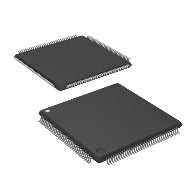
The device is supplied in P/PG-LBGA-160-1 package (P/PG-LBGA-160-1 is RoHS compliant) and in a PG-TQFP144-17 package, and is designed to minimize the number of external components required, so reducing system
costs and board space.
Due to its multitude of implemented functions, it fits to a wide range of networking applications and fulfills the
according international standards.
Crystal-less jitter attenuation with only one master clock source reduces the amount of required external
components.
Equipped with a flexible microprocessor interface, a SCI and a SPI interface, it connects to various control
processor environment. A standard boundary scan interface is provided to support board level testing. LBGA
device packaging, minimum number of external components and low power consumption lead to reduced overall
system costs.
The QuadLIUTM is not hardware and software compatibel to older versions!
Other members of the FALC® family are the OctalLIUTM supporting eight line interface components on a single
chip, the OctalFALCTM and the QuadFALC® E1/T1/J1 Framer And Line interface Components for long-haul and
short-haul applications, supporting 8 or 4 channels on a single chip respectively.
Data Sheet
12
Rev. 1.3, 2006-01-25
�Quad E1/T1/J1 Line Interface Component for Longand Short-Haul Applications
QuadLIUTM
PEF 22504 E
Version 2.1
1.1
Features
Line Interface
•
•
•
•
•
•
•
•
•
•
•
•
•
•
•
•
•
•
•
•
•
•
•
•
•
•
High-density, generic interface for all E1/T1/J1 applications
Four Analog receive and transmit circuits for long-haul and short-haul
applications
E1 or T1/J1 mode selectable
Data and clock recovery using an integrated digital phase-locked loop
P/PG-LBGA-160-1
Clock generator for jitter-free transmit clocks per channel
Jitter specifications of ITU-T I.431, G.703, G.736 (E1), G.823 (E1) and
AT&T TR62411 (T1/J1) and PUB 62411 are met
Maximum line attenuation up to -43 dB at 1024 kHz (E1) and up to 36 dB at 772 kHz (T1/J1)
Flexible programmable transmit pulse shapes for E1 and T1/J1 pulse
masks
Programmable line build-out for CSU signals according to ANSI T1.
403 and FCC68: 0 dB, -7.5 dB, -15 dB, -22.5 dB (T1/J1)
Programmable low transmitter output impedances for high transmit
return loss and generic E1/T1/J1 applications
Tristate function of the analog transmit line outputs
P-TQFP-144-6, -8, -14
Transmit line monitor protecting the device from damage
Flexible tristate functions of the digital receive outputs
Receive line monitor mode
Integrated switchtable 300 Ω receive resistors for generic E1/T1/J1
applications to meet termination resistance 75/120 Ω for E1, 100 Ω for T1 and 110 Ω for J1
Integrated multi purpose analog switch at line receive interface to support generic redundancy applications
(only supported in P/PG-LBGA-160-1 package)
Crystal-less wander and jitter attenuation/compensation according to TR 62411, ETS-TBR 12/13, PUB 62411
Common master clock reference for E1 and T1/J1 with any frequency within 1.02 and 20 MHz
Power-down function
Support of automatic protection switching
Dual-rail or single-rail digital inputs and outputs
Unipolar CMI for interfacing fiber-optical transmission routes
Selectable line codes (E1: HDB3, AMI/T1: B8ZS, AMI with ZCS)
Loss-of-signal indication with programmable thresholds according to ITU-T G.775, ETS300233 (E1) and ANSI
T1.403 (T1/J1)
Optional data stream muting upon LOS detection
Programmable receive slicer threshold
Type
Package
PEF 22504 HT
PG-TQFP-144-17
PEF 22504 E
P/PG-LBGA-160-1
Data Sheet
13
Rev. 1.3, 2006-01-25
�QuadLIUTM
PEF 22504
Introduction
•
•
•
•
•
•
•
•
•
•
•
Local loop, digital loop and remote loop for diagnostic purposes. Automatic remote loop switching is possible
with In-Band and Out-Band loop codes
Low power device, two power supply voltages 1.8 V and 3.3 V or a single supply of 3.3 V
Alarm and performance monitoring per second 16-bit counter for code violations, PRBS bit errors
Insertion and extraction of alarm indication signals (AIS)
Single-bit defect insertion
Flexible clock frequency for receiver and transmitter
Dual elastic stores for both, receive and transmit route clock wander and jitter compensation; controlled slip
capability and slip indication
Programmable elastic buffer size: 2 frames/1 frame/short buffer/bypass
Programmable In-band loop code detection and generation (TR62411)
Local loop back, payload loop back land remote loop back capabilities (TR54016)
Flexible pseudo-random binary sequence generator and monitor
Microprocessor Interfaces
•
•
•
•
•
•
•
•
Asynchronous 8/16-bit microprocessor bus interface (Intel or Motorola type selectable)
SPI bus interface
SCI bus interface
All registers directly accessible
Multiplexed and non-multiplexed address bus operations on asynchronous 8/16-bit microprocessor bus
interface
Hard/software reset options
Extended interrupt capabilities
One-second timer (internal or external timing reference)
General
•
•
•
•
•
Boundary scan standard IEEE 1149.1
PG-TQFP-144-17P-BGA-160-1 package
Temperature range from -40 to +85 °C
1.8 V and 3.3 V power supply or single 3.3 V power supply
Typical power consumption 140 mW per channel
Applications
•
•
•
•
•
•
•
•
Wireless base stations
E1/T1/J1 ATM gateways, multiplexer
E1/T1/J1 Channel & Data Service Units (CSU, DSU)
E1/T1/J1 Internet access equipment
LAN/WAN router
ISDN PRI, PABX
Digital Access Crossconnect Systems (DACS)
SONET/SDH add/drop multiplexer
Data Sheet
14
Rev. 1.3, 2006-01-25
�QuadLIUTM
PEF 22504
Introduction
MCLK
SYNC
FSC
RES
INT
READY/TDACK
BHE/BLE
ALE
DBW
(SCI- or
Microprocessor Interface
SPI-Bus)
Receive
Digital
Interface
XDI(4:1)
XPA(4:1)
XPB(4:1)
XPC(4:1)
XPD(4:1)
FCLKX(4:1)
Transmit
Digital
Interface
IM(1:0)
VSS
WR/RW
RD/DS
CS
XL1(4:1)
XL2(4:1)
RDO(4:1)
RPA(4:1)
RPB(4:1)
RPC(4:1)
RPD(4:1)
FCLKR(4:1)
READY_EN
TDI
TMS
TCK
TRS
TDO
VDDX(1:4)
Transmit
Line
Interface
QuadLIU V2.1
PEF 22504 E
P/PG-BGA-160-1
PEF 22504 HT
PG-TQFP-144-17
A(9:0)
Boundary
Scan
Interface
RLAS2(4:1)
RL1(4:1)
RL2(4:1)
D(15:0)/SCI
Receive
Line
Interface
VSEL
VDDC
VDDP
VDDPLL
Logic Symbol
VDDR(1:4)
1.2
Mode
QLIU_Logic_symbol
Figure 1
Data Sheet
Logic Symbol
15
Rev. 1.3, 2006-01-25
�QuadLIUTM
PEF 22504
Introduction
1.3
Typical Applications
Figure 2 shows a multiple link application, Figure 3 a repeater application using the QuadLIUTM.
4 x E1/T1/J1
Receive &
Transmit
.
.
.
QuadLIU
PEB 22504
System
Highway
Framer ASIC
Microprocessor
QLIU_F0195
Figure 2
Typical Multiple Link Application
RL1.1
RDO1
FCLKR1
Bidirectional
Line #1
RL2.1
RDON1
XL1.1
XDI1
FCLKX1
XL2.1
RL1.2
1/2
QuadLIU
XDIN1
RDO2
FCLKR2
Bidirectional
Line #2
RL2.2
RDON2
XL1.2
XDI2
FCLKX2
XL2.2
XDIN2
QLIU_F0069
Figure 3
Data Sheet
Typical Multiple Repeater Application between line #1 and Line #2
16
Rev. 1.3, 2006-01-25
�QuadLIUTM
PEF 22504
Pin Descriptions
2
Pin Descriptions
In this chapter the function and placement of all pins are described.
2.1
Ball Diagram P/PG-LBGA-160-1 (top view)
Figure 4 shows the ball layout of the QuadLIUTM in a P/PG-LBGA-160-1 package.
1
2
3
4
6
7
8
9
10
11
12
13
14
XL1_2 XL2_2 VDDR VSSR RL1_2 RL2_2 RL2_1 RL1_1 VSSR VDDR XL2_1 XL1_1
A
VSSX
B (RLAS22) VSSX
XDI1
FCLKX
1
MCLK XPC2
C
VDDX VDDX
D
RPC1
RPA1
E
RDO1
FCLKR
VDD
1
F
RDO2
VSS
FCLKR
RPA2
2
G
RPC2
RPB2
FCLKX
RPD2
2
H
XDI3
FCLKX
XDI2
3
J
RPB3 RPD3 RPC3
K
RDO3
L
5
M
RPB1 RPD1
IM1
VDD
(VSS)
FCLKR
RPB4
4
RPA4
VDDX VDDX RPC4
VSSX
N (RLAS23) VSSX
P
TCK
RPD4
TRS
XPD2
VDD
XPA1 VDDP XPB1
VSSX
(RLAS21)
D15
VSSX
VDDX VDDX
VSSP VDDP XPA2
XPB2 XPC1 VDDC
TDO
D14
TMS
VSS
TDI
D12
D13
D11
VSS
VDD
VDD
D10
D9
D7
D8
D6
VSEL RCLK2
XPD1 RCLK1
VDD
RPA3
VSS
VSS
D5
VSS
VSS
D2
READY
/DTACK D4
(VDD)
READY_
D0
EN
(VSS)
D3
D1
FCLKR
3
BHE/
BLE
CS
WR/
RW
RD/DS
RDO4
A9
A8
A6
A7
SEC/
FSC
A5
A3
A2
A4
XPD4 VDDC
IM
A1
VDDX VDDX
XPC4
A0
VSSX
DBW RCLK3 XPA3 XPD3
FCLKX
4
INT
RES
VDD
XDI4
XPC3 SYNC XPB3
XPB4
VDD
ALE
XPA4 RCLK4
VSS
VSSX
(RLAS24)
XL1_3 XL2_3 VDDR VSSR RL1_3 RL2_3 RL2_4 RL1_4 VSSR VDDR XL2_4 XL1_4
QLIU_F0213_2
Figure 4
Top View of the Pin Configuration (Ball Layout) P/PG-LBGA-160-1
2.2
Ball Diagram P/PG-LBGA-160-1 (bottom view)
Figure 4 shows the ball layout of the QuadLIUTM in a P/PG-LBGA-160-1 package.
Data Sheet
17
Rev. 1.3, 2006-01-25
�QuadLIUTM
PEF 22504
Pin Descriptions
14
A
13
12
11
10
9
8
7
6
5
4
3
2
1
XL1_1 XL2_1 VDDR VSSR RL1_1 RL2_1 RL2_2 RL1_2 VSSR VDDR XL2_2 XL1_2
VSSX
B (RLAS21) VSSX
D15
XPB1 VDDP
C
D14
VDDX VDDX
TRS
XPC2 MCLK
XDI1
VSSX
VSSX
(RLAS22)
XPA1
VDD
XPD2
TDO
VDDC XPC1
XPB2
XPA2 VDDP VSSP
TCK
FCLKX
VDDX VDDX
1
RCLK1 XPD1
VSS
RCLK2 VSEL
RPD1
RPB1 RPA1
VDD
D
D11
D13
D12
TDI
E
D10
VDD
VDD
VSS
VDD
F
D6
D8
D7
D9
RPA2
FCLKR
VSS
2
RDO2
G
D3
D4
FCLKX
RPB2
2
RPC2
H
D1
D0
FCLKX
3
XDI3
J
RD/DS
WR/
RW
CS
BHE/
BLE
FCLKR
RPC3 RPD3
3
RPB3
K
A7
A6
A8
A9
L
A4
A2
A3
A5
SEC/
FSC
A1
IM
VDDC XPD4
A0
XPC4
M
VDDX VDDX
VSSX
N (RLAS24) VSSX
P
READY/
DTACK D5
(VDD)
READY_
D2
EN
(VSS)
TMS
VSS
VSS
RPD2
VSS
VSS
RPA3
RDO4
ALE
XDI2
VDD
RPC1
FCLKR
RDO1
1
IM1
RDO3
(VSS)
FCLKR
4
XPB4 XPD3
XPA3 RCLK3 DBW
RPA4 RPB4
VDD
FCLKX
RES
4
INT
RPC4 VDDX VDDX
XDI4
RPD4 VSSX
VSS RCLK4 XPA4
VDD
XPB3 SYNC XPC3
VSSX
(RLAS23)
XL1_4 XL2_4 VDDR VSSR RL1_4 RL2_4 RL2_3 RL1_3 VSSR VDDR XL2_3 XL1_3
QLIU_F0213_3
Figure 5
Data Sheet
Bottom View of the Pin Configuration (Ball Layout) P/PG-LBGA-160-1
18
Rev. 1.3, 2006-01-25
�QuadLIUTM
PEF 22504
Pin Descriptions
2.3
Pin Diagram P-TQFP-144
VSSX
D15
D14
D13
D12
D11
VSS
VDD
D10
D9
D8
D7
D6
D5
D4
D3
READY_EN (VSS)
READY/DTACK (VDD)
D2
D1
D0
BHE/BLE
CS
RD/DS
WR/RW
A9
A8
A7
A6
A5
A4
A3
A2
A1
A0
VSSX
Figure 6 shows the pin diagram of the QuadLIUTM.
108
109
104
100
96
92
88
84
80
76
73
72
112
68
116
64
120
60
124
56
128
52
132
48
136
44
140
40
144
1
4
8
12
16
20
24
28
32
37
36
VSSX
XDI1
SXLKX1
RPA1
RPB1
RPC1
RPD1
SCLKR1
RDO1
VDD
VSS
RDO2
SCLKR2
RPA2
RPB2
RPC2
RPD2
XDI2
SCLKX2
XDI3
SCLKX3
RPA3
RPB3
RPC3
RPD3
SCLKR3
RDO3
VDD
IM1 (VSS)
RDO4
SCLKR4
RPA4
RPB4
RPC4
RPD4
VSSX
XL1_1/XDOP1/XOID1
VDDX
XL2_1/XDON1/XFM1
TDI
TDO
VDDR
RL1_1/RDIP1/ROID1
RL2_1/RDIN1/RCLKI1
VSSR
VDDC
RCLK1
XPA1
XPB1
XPC1
XPD1
VDDP
VSS
XPA2
XPB2
XPC2
XPD2
RCLK2
TRS
VDDP
MCLK
VSEL
VSSP
VSSR
RL2_2/RDIN2/RCLKI2
RL1_2/RDIP2/ROID2
VDDR
TCK
TMS
XL2_2/XDON2/XFM2
VDDX
XL1_2/XDOP2/XOID2
Figure 6
Data Sheet
XL1_4/XDOP4/XOID4
VDDX
XL2_4/XDON4/XFM4
SEC/FSC
IM
VDDR
RL1_4/RDIP4/ROID4
RL2_4/RDIN4/RCLKI4
VSSR
VDDC
ALE
RCLK4
XPD4
XPC4
XPB4
XPA4
VSS
VDD
XPD3
XPC3
XPB3
XPA3
SCLKX4
XDI4
SYNC
RCLK3
RES
VSSR
RL2_3/RDIN3/RCLKI3
RL1_3/RDIP3/ROID3
VDDR
INT
DBW
XL2_3/XDON3/XFM3
VDDX
XL1_3/XDOP3/XOID3
QLIU_F214
Pin Configuration P-TQFP-144-8
19
Rev. 1.3, 2006-01-25
�QuadLIUTM
PEF 22504
Pin Descriptions
2.4
Pin Definitions and Functions
The following table describes all pins and their functions:
Table 1
Pin No.
I/O Signals for P/PG-LBGA-160-1
Name
Pin Type Buffer
Type
Function
Operation Mode Selection and Device Initialization
M5
RES
I
PU
Hardware Reset
Active low
Interface Mode Selection
´00B´: Asynchronous Intel Bus Mode.
´01B´: Asynchronous Motorola Bus Mode
´10B´: SPI Bus Slave Mode.
´11B´: SCI Bus Slave Mode
K2
IM1
I
PD
M11
IM0
I
PU
Asynchronous and Serial Micro Controller Interfaces
K11
A9
I
PU
Address Bus Line 9 (MSB)
K12
A8
I
PU
Address Bus Line 8
K14
A7
I
PU
Address Bus Line 7
K13
A6
I
PU
Address Bus Line 6
L11
A5
I
PU
Address Bus Line 5
A5
I
PU
SCI source address bit 5 (MSB)
Only used if SCI interface mode is selected by IM(1:0) =
´11b´.
A4
I
PU
Address Bus Line 4
A4
I
PU
SCI source address bit 4
Only used if SCI interface mode is selected by IM(1:0) =
´11b´.
A3
I
PU
Address Bus Line 3
A3
I
PU
SCI source address bit 3
Only used if SCI interface mode is selected by IM(1:0) =
´11b´.
A2
I
PU
Address Bus Line 2
A2
I
PU
SCI source address bit 2
Only used if SCI interface mode is selected by IM(1:0) =
´11b´.
A1
I
PU
Address Bus Line 1
A1
I
PU
SCI source address bit 1
Only used if SCI interface mode is selected by IM(1:0) =
´11b´.
A0
I
PU
Address Bus Line 0
A0
I
PU
SCI source address bit 0 (LSB)
Only used if SCI interface mode is selected by IM(1:0) =
´11b´.
D15
IO
PU
Data Bus Line 15
PLL10
I
PU
PLL programming bit 10
Only used if SCI or SPI interface mode is selected by
IM(1:0) = ´1Xb´.
L14
L12
L13
M12
N12
B12
Data Sheet
20
Rev. 1.3, 2006-01-25
�QuadLIUTM
PEF 22504
Pin Descriptions
Table 1
I/O Signals (cont’d)for P/PG-LBGA-160-1
Pin No.
Name
Pin Type Buffer
Type
Function
C12
D14
IO
PU
Data Bus Line 14
PLL9
I
PU
PLL programming bit 9
Only used if SCI or SPI interface mode is selected by
IM(1:0) = ´1Xb´.
D13
IO
PU
Data Bus Line 13
PLL8
I
PU
PLL programming bit 8
Only used if SCI or SPI interface mode is selected by
IM(1:0) = ´1Xb´.
D12
IO
PU
Data Bus Line 12
PLL7
I
PU
PLL programming bit 7
Only used if SCI or SPI interface mode is selected by
IM(1:0) = ´1Xb´.
D11
IO
PU
Data Bus Line 11
PLL6
I
PU
PLL programming bit 6
Only used if SCI or SPI interface mode is selected by
IM(1:0) = ´1Xb´.
D10
IO
PU
Data Bus Line 10
PLL5
I
PU
PLL programming bit 5
Only used if SCI or SPI interface mode is selected by
IM(1:0) = ´1Xb´.
D9
IO
PU
Data Bus Line 9
PLL4
I
PU
PLL programming bit 4
Only used if SCI or SPI interface mode is selected by
IM(1:0) = ´1Xb´.
D13
D12
D14
E14
F11
F13
D8
IO
PU
Data Bus Line 8
PLL3
I
PU
PLL programming bit 3
Only used if SCI or SPI interface mode is selected by
IM(1:0) = ´1Xb´.
D7
IO
PU
Data Bus Line 7
PLL2
I
PU
PLL programming bit 2
Only used if SCI or SPI interface mode is selected by
IM(1:0) = ´1Xb´.
D6
IO
PU
Data Bus Line 6
PLL1
I
PU
PLL programming bit 1
Only used if SCI or SPI interface mode is selected by
IM(1:0) = ´1Xb´.
D5
IO
PU
Data Bus Line 5
PLL0
I
PU
PLL programming bit 0
Only used if SCI or SPI interface mode is selected by
IM(1:0) = ´1Xb´.
G13
D4
IO
PU
Data Bus Line 4
G14
D3
IO
PU
Data Bus Line 3
F12
F14
G11
Data Sheet
21
Rev. 1.3, 2006-01-25
�QuadLIUTM
PEF 22504
Pin Descriptions
Table 1
I/O Signals (cont’d)for P/PG-LBGA-160-1
Pin No.
Name
Pin Type Buffer
Type
Function
H11
D2
IO
PU
Data Bus Line 2
SCI_CLK
I
–
SCI Bus Clock
Only used if SCI interface mode is selected by IM(1:0) =
´11b´.
SCLK
I
–
SPI Bus Clock
Only used if SPI interface mode is selected by IM(1:0) =
´10b´.
D1
IO
PU
Data Bus Line 1
SCI_RXD
I
PU
SCI Bus Serial Data In
Only used if SCI interface mode is selected by IM(1:0) =
´11b´.
SDI
I
PU
SPI Serial Data In
Only used if SPI interface mode is selected by IM(1:0) =
´10b´.
D0
IO
PU
Data Bus Line 0
SCI_TXD
I
PP or oD SCI Bus Serial Data Out
Only used if SCI interface mode is selected by IM(1:0) =
´11b´.
SDO
I
PU
SPI Bus Serial Data Out
Only used if SPI interface mode is selected by IM(1:0) =
´10b´.
L9
ALE
I
PU
Address Latch Enable
A high on this line indicates an address on an external
multiplexed address/data bus. The address information
provided on lines A(10:0) is internally latched with the
falling edge of ALE. This function allows the QuadLIUTM
to be connected to a multiplexed address/data bus
without the need for external latches. In this case, pins
A(7:0) must be connected to the data bus pins
externally. In case of demultiplexed mode this pin can
be connected directly to VDD or can be left open.
J14
RD
I
PU
Read Enable
Intel bus mode.
This signal indicates a read operation. When the
QuadLIUTM is selected via CS, the RD signal enables
the bus drivers to output data from an internal register
addressed by A(10:0) to the Data Bus.
DS
I
PU
Data Strobe
Motorola bus mode.
This pin serves as input to control read/write operations.
H14
H13
Data Sheet
22
Rev. 1.3, 2006-01-25
�QuadLIUTM
PEF 22504
Pin Descriptions
Table 1
I/O Signals (cont’d)for P/PG-LBGA-160-1
Pin No.
Name
Pin Type Buffer
Type
Function
J13
WR
I
PU
Write Enable
Intel bus mode.
This signal indicates a write operation. When CS is
active the QuadLIUTM loads an internal register with
data provided on the data bus.
RW
I
PU
Read/Write Select
Motorola bus mode.
This signal distinguishes between read and write
operation.
L4
DBW
I
PU
Data Bus Width select
Bus interface mode
A low signal on this input selects the 8-bit bus interface
mode. A high signal on this input selects the 16-bit bus
interface mode. In this case word transfer to/from the
internal registers is enabled. Byte transfers are
implemented by using A0 and BHE/BLE.
J11
BHE
I
PU
Bus High Enable
Intel bus mode.
If 16-bit bus interface mode is enabled, this signal
indicates a data transfer on the upper byte of the data
bus D(15:8). In 8-bit bus interface mode this signal has
no function and should be tied to VDD or left open.
BLE
I
PU
Bus Low Enable
Motorola bus mode.
If 16-bit bus interface mode is enabled, this signal
indicates a data transfer on the lower byte of the data
bus D(7:0). In 8-bit bus interface mode this signal has
no function and should be tied to VDD or left open.
J12
CS
I
PU
Chip Select
Low active chip select.
M4
INT
O
–
Interrupt Request
Interrupt request.
INT serves as general interrupt request for all interrupt
sources. These interrupt sources can be masked via
registers IMR(7:0). Interrupt status is reported via
registers GIS (Global Interrupt Status) and ISR(7:0).
Output characteristics (push-pull active low/high, open
drain) are determined by programming register IPC.
Data Sheet
23
Rev. 1.3, 2006-01-25
�QuadLIUTM
PEF 22504
Pin Descriptions
Table 1
I/O Signals (cont’d)for P/PG-LBGA-160-1
Pin No.
Name
Pin Type Buffer
Type
Function
G12
READY
O
oD
(PU)
Data Ready
oD output only if activated by READY_EN = 1B and if
Intel bus mode is selected. If not activated (READY_EN
= 0B) the pull-up resistor is active.
Asynchronous handshake signal to indicate successful
read or write cycle.
DTACK
O
oD
(PU)
Data Acknowledge
oD output only if activated by READY_EN = 1B and if
motorola bus mode is selected. If not activated
(READY_EN = 0B) the pull-up resistor is active.
Asynchronous handshake signal to indicate successful
read or write cycle.
READY_EN
I
PD
Ready Enable
Activates the oD functionality of READY/ DTACK.
0B: READY/ DTACK is not activated (only pull-up
resistor is active). Pin READY/ DTACK can be
connected to VDD.
1B: READY/ DTACK is an active oD output
H12
Separate Analog Switches (only supported in BGA package)
B14
RLAS21
IO
(analog)
–
Analog Switch Connector port 1
Can be connected to VSSX if analog switch is not used
(HW compatibel to QuadFALC® v2.1)
B1
RLAS22
IO
(analog)
–
Analog Switch Connector port 2
Can be connected to VSSX if analog switch is not used
(HW compatibel to QuadFALC® v2.1)
N1
RLAS23
IO
(analog)
–
Analog Switch Connector port 3
Can be connected to VSSX if analog switch is not used
(HW compatibel to QuadFALC® v2.1)
N14
RLAS24
IO
(analog)
–
Analog Switch Connector port 4
Can be connected to VSSX if analog switch is not used
(HW compatibel to QuadFALC® v2.1)
RL1.1
I (analog) –
Line Receiver input 1, port 1
Analog input from the external transformer. Selected if
LIM1.DRS is cleared.
ROID1
I
–
Receive Optical Interface Data, port 1
Unipolar data received from a fiber-optical interface with
2048 kbit/s (E1) or 1544 kbit/s (T1/J1). If CMI coding is
selected (MR0.RC(1:0) = ´01b´ and LIM0.DRS = ´1´), an
internal DPLL recovers clock an data; no clock signal on
RCLKI2 is required.
RL2.1
I (analog) –
Line Receiver input 2, port 1
Analog input from the external transformer. Selected if
LIM1.DRS is cleared.
Line Interface Receiver
A9
A8
Data Sheet
24
Rev. 1.3, 2006-01-25
�QuadLIUTM
PEF 22504
Pin Descriptions
Table 1
I/O Signals (cont’d)for P/PG-LBGA-160-1
Pin No.
Name
Pin Type Buffer
Type
Function
A6
RL1.2
I (analog) –
Line Receiver input 1, port 1
Analog input from the external transformer. Selected if
LIM1.DRS is cleared.
ROID2
I
–
Receive Optical Interface Data, port 2
Unipolar data received from a fiber-optical interface with
2048 kbit/s (E1) or 1544 kbit/s (T1/J1). If CMI coding is
selected (MR0.RC(1:0) = ´01b´ and LIM0.DRS = ´1´), an
internal DPLL recovers clock an data; no clock signal on
RCLKI2 is required.
A7
RL2.2
I (analog) –
Line Receiver input 2, port 2
Analog input from the external transformer. Selected if
LIM1.DRS is cleared.
P6
RL1.3
I (analog) –
Line Receiver input 1, port 3
Analog input from the external transformer. Selected if
LIM1.DRS is cleared.
ROID3
I
–
Receive Optical Interface Data, port 3
Unipolar data received from a fiber-optical interface with
2048 kbit/s (E1) or 1544 kbit/s (T1/J1). If CMI coding is
selected (MR0.RC(1:0) = ´01b´ and LIM0.DRS = ´1´), an
internal DPLL recovers clock an data; no clock signal on
RCLKI2 is required.
P7
RL2.3
I (analog) –
Line Receiver input 2, port 3
Analog input from the external transformer. Selected if
LIM1.DRS is cleared.
P9
RL1.4
I (analog) –
Line Receiver input 1, port 4
Analog input from the external transformer. Selected if
LIM1.DRS is cleared.
ROID4
I
–
Receive Optical Interface Data, port 4
Unipolar data received from a fiber-optical interface with
2048 kbit/s (E1) or 1544 kbit/s (T1/J1). If CMI coding is
selected (MR0.RC(1:0) = ´01b´ and LIM0.DRS = ´1´), an
internal DPLL recovers clock an data; no clock signal on
RCLKI2 is required.
RL2.4
I (analog) –
Line Receiver input 2, port 4
Analog input from the external transformer. Selected if
LIM1.DRS is cleared.
P8
Data Sheet
25
Rev. 1.3, 2006-01-25
�QuadLIUTM
PEF 22504
Pin Descriptions
Table 1
Pin No.
I/O Signals (cont’d)for P/PG-LBGA-160-1
Name
Pin Type Buffer
Type
Function
XL1.1
O
(analog)
–
Transmit Line 1, port 1
Analog output to the external transformer. Selected if
LIM1.DRS is cleared. After reset this pin is in highimpedance state until bit MR0.XC1 is set and
XPM2.XLT is cleared.
XOID1
O
–
Transmit Optical Interface Data, port 1
Data in CMI code is shifted out with 50% or 100% duty
cycle on both transitions of XCLK2 according to the CMI
coding. Output polarity is selected by bit LIM0.XDOS
(after reset: data is sent active high). The single-rail
mode is selected if LIM1.DRS is set and MR0.XC1 is
cleared. After reset this pin is in high-impedance state
until register LIM1.DRS is set and XPM2.XLT is cleared.
A12
XL2.1
O
(analog)
–
Transmit Line 2, port 1
Analog output for the external transformer. Selected if
LIM1.DRS is cleared. After reset this pin is in highimpedance state until bit MR0.XC1 is set and
XPM2.XLT is cleared.
A2
XL1.2
O
(analog)
–
Transmit Line 1, port 2
Analog output to the external transformer. Selected if
LIM1.DRS is cleared. After reset this pin is in highimpedance state until bit MR0.XC1 is set and
XPM2.XLT is cleared.
XOID2
O
–
Transmit Optical Interface Data, port 2
Data in CMI code is shifted out with 50% or 100% duty
cycle on both transitions of XCLK2 according to the CMI
coding. Output polarity is selected by bit LIM0.XDOS
(after reset: data is sent active high). The single-rail
mode is selected if LIM1.DRS is set and MR0.XC1 is
cleared. After reset this pin is in high-impedance state
until register LIM1.DRS is set and XPM2.XLT is cleared.
XL2.2
O
(analog)
–
Transmit Line 2, port 2
Analog output for the external transformer. Selected if
LIM1.DRS is cleared. After reset this pin is in highimpedance state until bit MR0.XC1 is set and
XPM2.XLT is cleared.
Line Interface Transmitter
A13
A3
Data Sheet
26
Rev. 1.3, 2006-01-25
�QuadLIUTM
PEF 22504
Pin Descriptions
Table 1
I/O Signals (cont’d)for P/PG-LBGA-160-1
Pin No.
Name
Pin Type Buffer
Type
Function
P2
XL1.3
O
(analog)
–
Transmit Line 1, port 3
Analog output to the external transformer. Selected if
LIM1.DRS is cleared. After reset this pin is in highimpedance state until bit MR0.XC1 is set and
XPM2.XLT is cleared.
XOID3
O
–
Transmit Optical Interface Data, port 3
Data in CMI code is shifted out with 50% or 100% duty
cycle on both transitions of XCLK3 according to the CMI
coding. Output polarity is selected by bit LIM0.XDOS
(after reset: data is sent active high). The single-rail
mode is selected if LIM1.DRS is set and MR0.XC1 is
cleared. After reset this pin is in high-impedance state
until register LIM1.DRS is set and XPM2.XLT is cleared.
P3
XL2.3
O
(analog)
–
Transmit Line 2, port 3
Analog output for the external transformer. Selected if
LIM1.DRS is cleared. After reset this pin is in highimpedance state until bit MR0.XC1 is set and
XPM2.XLT is cleared.
P13
XL1.4
O
(analog)
–
Transmit Line 1, port 4
Analog output to the external transformer. Selected if
LIM1.DRS is cleared. After reset this pin is in highimpedance state until bit MR0.XC1 is set and
XPM2.XLT is cleared.
XOID4
O
–
Transmit Optical Interface Data, port 4
Data in CMI code is shifted out with 50% or 100% duty
cycle on both transitions of XCLK4 according to the CMI
coding. Output polarity is selected by bit LIM0.XDOS
(after reset: data is sent active high). The single-rail
mode is selected if LIM1.DRS is set and MR0.XC1 is
cleared. After reset this pin is in high-impedance state
until register LIM1.DRS is set and XPM2.XLT is cleared.
XL2.4
O
(analog)
–
Transmit Line 2, port 4
Analog output for the external transformer. Selected if
LIM1.DRS is cleared. After reset this pin is in highimpedance state until bit MR0.XC1 is set and
XPM2.XLT is cleared.
MCLK
I
–
Master Clock
A reference clock of better than ±32 ppm accuracy in
the range of 1.02 to 20 MHz must be provided on this
pin. The QuadLIUTM internally derives all necessary
clocks from this master
(see registers GCM(6:1)).
P12
Clock Signals
B4
Data Sheet
27
Rev. 1.3, 2006-01-25
�QuadLIUTM
PEF 22504
Pin Descriptions
Table 1
I/O Signals (cont’d)for P/PG-LBGA-160-1
Pin No.
Name
Pin Type Buffer
Type
Function
N6
SYNC
I
PU
Clock Synchronization of DCO-R
If a clock is detected on pin SYNC the
DCO-R circuitry of the QuadLIUTM synchronizes to this
1.544/2.048 MHz clock (see LIM0.MAS, CMR1.DCS
and CMR2.DCF). Additionally, in master mode the
QuadLIUTM is able to synchronize to an 8 kHz reference
clock (IPC.SSYF = ´1´). If not connected, an internal
pull-up transistor ensures high input level.
FSC
O
–
8 kHz Frame Synchronization
The optionally synchronization pulse is active high or
low for one 2.048/1.544 MHz cycle (pulse width =
488 ns for E1and 648 ns or T1/J1).
RCLK(1:4)
O
–
Receive Clock Out, ports 1 to 4
After reset this ports are configured to be internally
pulled up weakly. Setting of register bit PC5.CRPR will
switch this ports to be active outputs.
L10
D10, D7, L5, N9
Digital (Framer) Interface Receive
E1
RDO1
O
–
Receive Data Out, port 1
Received data at RL1, RL2 is sent to RDOP, RDON.
Clocking of data is done with the rising or falling edge of
RCLK.
E2
FCLKR1
I/O
PU
Framer Data Clock Receive, port 1
Input if PC5.CSRP = ´0´, output if PC5.CSRP = ´1´.
F1
RDO2
O
–
Receive Data Out, port 2
See description of RDOP1.
F3
FCLKR2
I/O
PU
Framer Data Clock Receive, port 2
See description of FCLKR1.
K1
RDO3
O
–
Receive Data Out, port 3
See description of RDOP1.
J4
FCLKR3
I/O
PU
Framer Data Clock Receive, port 3
See description of FCLKR1.
K4
RDO4
O
–
Receive Data Out, port 4
See description of RDOP1.
L1
FCLKR4
I/O
PU
Framer Data Clock Receive, port 4
See description of FCLKR1.
Digital (Framer) Interface Transmit
B3
XDI1
I
–
Transmit Data In, port 1
NRZ transmit data received from the framer. Latching of
data is done with rising or falling transitions of FCLKX1
according to bit DIC3.RESX.
C3
FCLKX1
I/O
–
Framer Data Clock Transmit, port 1
H3
XDI2
I
–
Transmit Data In, port 2
See description of XDI1.
G3
FCLKX2
I/O
–
Framer Data Clock Transmit, port 2
See description of FCLKX1.
H1
XDI3
I
–
Transmit Data In, port 3
See description of XDI1.
Data Sheet
28
Rev. 1.3, 2006-01-25
�QuadLIUTM
PEF 22504
Pin Descriptions
Table 1
I/O Signals (cont’d)for P/PG-LBGA-160-1
Pin No.
Name
Pin Type Buffer
Type
Function
H2
FCLKX3
I/O
–
Framer Data Clock Transmit, port 3
See description of FCLKX1.
N4
XDI4
I
–
Transmit Data In, port 4
See description of XDI1.
M6
FCLKX4
I/O
–
Framer Data Clock Transmit, port 4
See description of FCLKX1.
I/O
PU/–
Receive Multifunction Pins A to D, port 1
Depending on programming of bits PC(1:4).RPC(3:0)
these multifunction ports carry information to the framer
interface or from the framer to the QuadLIUTM. After
reset these ports are configured to be inputs. With the
selection of the appropriate pin function, the
corresponding input/output configuration is achieved
automatically. Depending on bit DIC3.RESR
latching/transmission of data is done with the rising or
falling edge of FCLKR. If not connected, an internal pullup transistor ensures a high input level.
An input function must not be selected twice or more.
Selectable pin functions are described below.
I
PU
Receive Line Termination (RLT), port 1
PC(1:4).RPC(3:0) = ´1000b´.
These input function controls together with LIM0.RTRS
the analog switch of the receive line interface: A logical
equivalence is build out of LIM0.RTRS and RLT.
I
PU
General Purpose Input (GPI), port 1
PC(1:4).RPC(3:0) = ´1001b.
The pin is set to input. The state of this input is reflected
in the register bits MFPI.RPA, MFPI.RPB or MFPI.RPC
respectively.
O
–
General Purpose Output High (GPOH), port 1
PC(1:4).RPC(3:0) = ´1010b´.
The pin level is set fix to high level.
O
–
General Purpose Output Low (GPOL), port 1
PC(1:4).RPC(3:0) = ´1011b´.
The pin level is set fix to low-level.
O
–
Loss of Signal Indication Output (LOS), port 1
PC(1:3).RPC(3:0) = ´1100b.
The output reflects the Loss of Signal status as readable
in LSR0.LOS.
Multi Function Pins
D2
RPA1
D3
RPB1
D1
RPC1
D4
RPD1
D2
RPA1
D3
RPB1
D1
RPC1
D4
RPD1
D2
RPA1
D3
RPB1
D1
RPC1
D4
RPD1
D2
RPA1
D3
RPB1
D1
RPC1
D4
RPD1
D2
RPA1
D3
RPB1
D1
RPC1
D4
RPD1
D2
RPA1
D3
RPB1
D1
RPC1
D4
RPD1
Data Sheet
29
Rev. 1.3, 2006-01-25
�QuadLIUTM
PEF 22504
Pin Descriptions
Table 1
I/O Signals (cont’d)for P/PG-LBGA-160-1
Pin No.
Name
Pin Type Buffer
Type
Function
D2
RPA1
O
–
D3
RPB1
D1
RPC1
D4
RPD1
Receive Data Output Negative (RDON), port 1
PC(1:4).RPC(3:0) = ´1110b´.
Receive data output negative for dual rail mode on
digital (framer) interface (LIM3.DRR = ´1´).
Bipolar violation output for single rail mode on digital
(framer) interface (LIM3.DRR = ´0´).
D2
RPA1
O
–
D3
RPB1
D1
RPC1
D4
RPD1
Receive Clock Output (RCLK), port 1
PC(1:4).RPC(3:0) = ´1111b´. Default setting after reset
Receive clock output RCLK. After reset RCLK is
configured to be internally pulled up weekly. By setting
of PC5.CRP RCLK is an active output.
RCLK source and frequency selection is made by
CMR1.RS(1:0) if COMP = ´1´ or by CMR4.RS(2:0) if
COMP = ´0´.
F4
RPA2
I/O
PU/–
G2
RPB2
G1
RPC2
G4
RPD2
Receive Multifunction Pins A to D, port 2
Depending on programming of bits PC(1:4).RPC(3:0)
these multifunction ports carry information to the framer
interface or from the framer to the QuadLIUTM. After
reset these ports are configured to be inputs. With the
selection of the appropriate pin function, the
corresponding input/output configuration is achieved
automatically. Depending on bit DIC3.RESR
latching/transmission of data is done with the rising or
falling edge of FCLKR. If not connected, an internal pullup transistor ensures a high input level.
An input function must not be selected twice or more.
Selectable pin functions as described for port 1.
H4
RPA3
I/O
PU/–
Receive Multifunction Pins A to D, port 3
Depending on programming of bits PC(1:4).RPC(3:0)
these multifunction ports carry information to the framer
interface or from the framer to the QuadLIUTM. After
reset these ports are configured to be inputs. With the
selection of the appropriate pin function, the
corresponding input/output configuration is achieved
automatically. Depending on bit DIC3.RESR
latching/transmission of data is done with the rising or
falling edge of FCLKR. If not connected, an internal pullup transistor ensures a high input level.
An input function must not be selected twice or more.
Selectable pin functions as described for port 1.
J1
RPB3
J3
RPC3
J2
RPD3
Data Sheet
30
Rev. 1.3, 2006-01-25
�QuadLIUTM
PEF 22504
Pin Descriptions
Table 1
I/O Signals (cont’d)for P/PG-LBGA-160-1
Pin No.
Name
Pin Type Buffer
Type
Function
L3
RPA4
I/O
PU/–
L2
RPB4
M3
RPC4
N3
RPD4
Receive Multifunction Pins A to D, port 4
Depending on programming of bits PC(1:4).RPC(3:0)
these multifunction ports carry information to the framer
interface or from the framer to the QuadLIUTM. After
reset these ports are configured to be inputs. With the
selection of the appropriate pin function, the
corresponding input/output configuration is achieved
automatically. Depending on bit DIC3.RESR
latching/transmission of data is done with the rising or
falling edge of FCLKR. If not connected, an internal pullup transistor ensures a high input level.
An input function must not be selected twice or more.
Selectable pin functions as described for port 1.
B9
XPA1
I/O
PU/–
B11
XPB1
C9
XPC1
D9
XPD1
Transmit Multifunction Pins A to D, port 1
Depending on programming of bits PC(1:4).XPC(3:0)
these multifunction ports carry information to the framer
interface or from the framer to the QuadLIUTM. After
reset the ports are configured to be inputs. With the
selection of the appropriate pin function, the
corresponding input/output configuration is achieved
automatically. Depending on bit DIC3.RESX
latching/transmission of data is done with the rising or
falling edge of FCLKX. If not connected, an internal pullup transistor ensures a high input level.
Each input function (TCLK, XDIN, XLT or XLT) may only
be selected once.
Selectable pin functions are described below.
B9
XPA1
I
PU
B11
XPB1
C9
XPC1
D9
XPD1
Transmit Clock (TCLK), port 1
PC(1:4).XPC(3:0) = ´0011b´
A 2.048/8.192 MHz (E1) or 1.544/6.176 MHz (T1/J1)
clock has to be sourced by the framer if the internally
generated transmit clock (generated by DCO-X) shall
not be used. Optionally this input is used as a
synchronization clock for the DCO-X circuitry with a
frequency of 2.048 (E1) or 1.544 MHz (T1/J1).
B9
XPA1
O
–
B11
XPB1
C9
XPC1
D9
XPD1
Transmit Clock (XCLK), port 1
PC(1:4).XPC(3:0) = ´0111b´
Transmit line clock of 2.048 MHz (E1) or 1.544 MHz
(T1/J1) derived from FCLKX/R, RCLK or generated
internally by DCO circuitries.
B9
XPA1
I
PU
B11
XPB1
C9
XPC1
D9
XPD1
Transmit Line Tristate (XLT), port 1
PC(1:4).XPC(3:0) = ´1000b´
A high level on this port sets the transmit lines XL1/2 or
XDOP/N into tristate mode. This pin function is logically
OR´d with register bit XPM2.XLT.
Data Sheet
31
Rev. 1.3, 2006-01-25
�QuadLIUTM
PEF 22504
Pin Descriptions
Table 1
I/O Signals (cont’d)for P/PG-LBGA-160-1
Pin No.
Name
Pin Type Buffer
Type
Function
B9
XPA1
I
PU
B11
XPB1
C9
XPC1
D9
XPD1
General Purpose Input (GPI), port 1
PC(1:4).XPC(3:0) = ´1001b.
The pin is set to input. The state of this input is reflected
in the register bits MFPI.XPA, MFPI.XPB or MFPI.XPC
respectively.
B9
XPA1
O
–
B11
XPB1
C9
XPC1
General Purpose Output High (GPOH), port 1
PC(1:4).XPC(3:0) = ´1010b´.
The pin level is set fix to high level.
D9
XPD1
B9
XPA1
O
–
B11
XPB1
C9
XPC1
General Purpose Output Low (GPOL), port 1
PC(1:4).XPC(3:0) = ´1011b´.
The pin level is set fix to high level.
D9
XPD1
B9
XPA1
I
PU
B11
XPB1
C9
XPC1
D9
XPD1
Transmit Data Input Negative (XDIN), port 1
PC(1:2).XPC(3:0) = ´1101b.
Transmit data input negative for dual rail mode on
framer side (LIM3.DRX = ´1´). Depending on bit
DIC3.RESX latching of data is done with the rising or
falling edge of FCLKX.
B9
XPA1
I
PU
B11
XPB1
C9
XPC1
D9
XPD1
Transmit Line Tristate, low active, port 1
XLT : PC(1:4).XPC(3:0) = ´1110b´.
A low level on this port sets the transmit lines XL1/2 or
XDOP/N into tristate mode. This pin function is logically
OR´d with register bit XPM2.XLT.
C7
C8
XPA2,
XPB2
I/O
PU/–
B5
XPC2
B7
XPD2
Transmit Multifunction Pins A to D, port 2
Depending on programming of bits PC(1:4).XPC(3:0)
these multifunction ports carry information to the framer
interface or from the framer to the QuadLIUTM. After
reset the ports are configured to be inputs. With the
selection of the appropriate pin function, the
corresponding input/output configuration is achieved
automatically. Depending on bit DIC3.RESX
latching/transmission of data is done with the rising or
falling edge of FCLKX. If not connected, an internal pullup transistor ensures a high input level.
Each input function (TCLK, XDIN, XLT or XLT) may only
be selected once.
Selectable pin functions as described for port 1.
Data Sheet
32
Rev. 1.3, 2006-01-25
�QuadLIUTM
PEF 22504
Pin Descriptions
Table 1
I/O Signals (cont’d)for P/PG-LBGA-160-1
Pin No.
Name
Pin Type Buffer
Type
Function
L6
N7
XPA3
XPB3
I/O
PU/–
N5
XPC3
L7
XPD3
Transmit Multifunction Pins A to D, port 3
Depending on programming of bits PC(1:4).XPC(3:0)
these multifunction ports carry information to the framer
interface or from the framer to the QuadLIUTM. After
reset the ports are configured to be inputs. With the
selection of the appropriate pin function, the
corresponding input/output configuration is achieved
automatically. Depending on bit DIC3.RESX
latching/transmission of data is done with the rising or
falling edge of FCLKX. If not connected, an internal pullup transistor ensures a high input level.
Each input function (TCLK, XDIN, XLT or XLT) may only
be selected once.
Selectable pin functions as described for port 1.
N8
L8
XPA4
XPB4
I/O
PU/–
N11
XPC4
M9
XPD4
Transmit Multifunction Pins A to D, port 4
Depending on programming of bits PC(1:4).XPC(3:0)
these multifunction ports carry information to the framer
interface or from the framer to the QuadLIUTM. After
reset the ports are configured to be inputs. With the
selection of the appropriate pin function, the
corresponding input/output configuration is achieved
automatically. Depending on bit DIC3.RESX
latching/transmission of data is done with the rising or
falling edge of FCLKX. If not connected, an internal pullup transistor ensures a high input level.
Each input function (TCLK, XDIN, XLT or XLT) may only
be selected once.
Selectable pin functions as described for port 1.
Power Supply
A11
VDDR1
S
–
Positive Power Supply
For the analog receiver 1 (3.3 V)
A4
VDDR2
S
–
Positive Power Supply
For the analog receiver 2 (3.3 V)
P4
VDDR3
S
–
Positive Power Supply
For the analog receiver 3 (3.3 V)
P11
VDDR4
S
–
Positive Power Supply
For the analog receiver 4 (3.3 V)
C13, C14
VDDX1
S
–
Positive Power Supply
For the analog transmitter 1
C1, C2
VDDX2
S
–
Positive Power Supply
For the analog transmitter 2
M1, M2
VDDX3
S
–
Positive Power Supply
For the analog transmitter 3
M13, M14
VDDX4
S
–
Positive Power Supply
For the analog transmitter 4
Data Sheet
33
Rev. 1.3, 2006-01-25
�QuadLIUTM
PEF 22504
Pin Descriptions
Table 1
I/O Signals (cont’d)for P/PG-LBGA-160-1
Pin No.
Name
Pin Type Buffer
Type
Function
M10, C10
VDDC
S
–
Positive Power Supply
For the digital core (1.8 V).
These pins can either be positive power supply input or
output, dependent on VSEL:
VSEL connected to VSS : 1.8 V power supply inputs,
require decoupling.
VSEL connected to VDD: 1.8 V outputs for decoupling to
VSS . These pins must not be used to supply external
devices.
B10
VDDPLL
S
–
Positive Power Supply
For the analog PLL
VDDP
S
–
Positive Power Supply
For the digital pads(3.3 V)
For correct operation, all VDDP pins have to be
connected to positive power supply.
VSS
S
–
Power Ground
Common for all sub circuits (0 V)
For correct operation, all VSS pins have to be connected
to ground.
B1, B14, N1, N14 VSS
S
–
Only for P/PG-LBGA-160-1 Package
Either usage as power ground or usage as connectors
RLAS2 of the analog switches
I + PU
–
Voltage Select
Enables the internal voltage regulator for 3.3 V only
operation mode if connected to VDD (recommended) or
left open.
Disables the internal voltage regulator for dual power
supply mode (1.8 V and 3.3 V) if connected to VSS.
C6
E3, E4
K3
M7, M8
E12, E13, B8
P5
P10
A10
A5
B2
N2
N13
B13
F2
N10
E11
D8
G7
G8
H7
H8
C5
Power Supply Configuration
D6
Data Sheet
VSEL
34
Rev. 1.3, 2006-01-25
�QuadLIUTM
PEF 22504
Pin Descriptions
Table 1
Pin No.
I/O Signals (cont’d)for P/PG-LBGA-160-1
Name
Pin Type Buffer
Type
Function
Boundary Scan/Joint Test Access Group (JTAG)
B6
TRS
D11
TDI
D5
TMS
Test Mode Select
For Boundary Scan.
If not connected an internal pull-up transistor ensures
high input level.
C4
TCK
Test Clock
For Boundary Scan.
If not connected an internal pull-up transistor ensures
high input level.
C11
TDO
I
O
PD
Test Reset
For Boundary Scan (active low). If not connected, an
internal pull-down transistor ensures low input level.
PU
Test Data Input
For Boundary Scan.
If not connected an internal pull-up transistor ensures
high input level.
–
Test Data Output
For Boundary Scan
Note: oD = open drain output PU = input or input/output comprising an internal pull-up device To override the
internal pull-up by an external pull-down, a resistor value of 22 kΩ is recommended. The pull-up devices are
activated during reset, this means their state is undefined until the reset signal has been applied. Unused
pins containing pull-ups can be left open.
Data Sheet
35
Rev. 1.3, 2006-01-25
�QuadLIUTM
PEF 22504
Pin Descriptions
Table 2
Pin No.
I/O Signals for P-TQFP-144-8
Name
Pin Type
Buffer
Type
Function
Operation Mode Selection and Device Initialization
46
RES
I
PU
Hardware Reset
Active low.
29
IM1
I
PD
68
IM
I
PU
Interface Mode Selection
00B Asynchronous Intel Bus Mode
01B Asynchronous Motorola Bus Mode
10B SPI Bus Slave Mode
11B SCI Bus Slave Mode
Asynchronous and Serial Microcontroller Interfaces
83
A9
I
PU
Address Bus Line 9 (MSB)
82
A8
I
PU
Address Bus Line 8
81
A7
I
PU
Address Bus Line 7
80
A6
I
PU
Address Bus Line 6
79
A5
I
PU
Address Bus Line 5
A5
I
PU
SCI Source address bit 5 (MSB)
Only used if SCI interface mode is selected by IM(1:0) = 11B.
A4
I
PU
Address Bus Line 4
A4
I
PU
SCI Source Address bit 4
Only used if SCI interface mode is selected by IM(1:0) = 11B.
A3
I
PU
Address Bus Line 3
A3
I
PU
SCI Source Address bit 3
Only used if SCI interface mode is selected by IM(1:0) = 11B.
A2
I
PU
Address Bus Line 2
A2
I
PU
SCI Source Address bit 2
Only used if SCI interface mode is selected by IM(1:0) = 11B.
A1
I
PU
Address Bus Line 1
A1
I
PU
SCI Source Address bit 1
Only used if SCI interface mode is selected by IM(1:0) = 11B.
A0
I
PU
Address Bus Line 0
A0
I
PU
SCI Source Address Bit 0 (LSB)
Only used if SCI interface mode is selected by IM(1:0) = 11B.
D15
IO
PU
Data Bus Line 15
PLL10
I
PU
PLL Programming Bit 10
Only used if SCI or SPI interface mode is selected by IM(1:0)
= 1XB.
78
77
76
75
74
107
106
105
D14
IO
PU
Data Bus Line 14
PLL9
I
PU
PLL Programming Bit 9
Only used if SCI or SPI interface mode is selected by IM(1:0)
= 1XB.
D13
IO
PU
Data Bus Line 13
PLL8
I
PU
PLL programming bit 8
Only used if SCI or SPI interface mode is selected by
IM(1:0) = 1XB.
Data Sheet
36
Rev. 1.3, 2006-01-25
�QuadLIUTM
PEF 22504
Pin Descriptions
Table 2
I/O Signals for P-TQFP-144-8 (cont’d)
Pin No.
Name
Pin Type
Buffer
Type
Function
104
D12
IO
PU
Data Bus Line 12
PLL7
I
PU
PLL programming bit 7
Only used if SCI or SPI interface mode is selected by
IM(1:0) = 1XB.
D11
IO
PU
Data Bus Line 11
PLL6
I
PU
PLL programming bit 6
Only used if SCI or SPI interface mode is selected by
IM(1:0) = 1XB.
103
100
99
98
97
96
D10
IO
PU
Data Bus Line 10
PLL5
I
PU
PLL programming bit 5
Only used if SCI or SPI interface mode is selected by
IM(1:0) = 1XB.
D9
IO
PU
Data Bus Line 9
PLL4
I
PU
PLL programming bit 4
Only used if SCI or SPI interface mode is selected by
IM(1:0) = 1XB.
D8
IO
PU
Data Bus Line 8
PLL3
I
PU
PLL programming bit 3
Only used if SCI or SPI interface mode is selected by
IM(1:0) = 1XB.
D7
IO
PU
Data Bus Line 7
PLL2
I
PU
PLL programming bit 2
Only used if SCI or SPI interface mode is selected by
IM(1:0) = 1XB.
D6
IO
PU
Data Bus Line 6
PLL1
I
PU
PLL programming bit 1
Only used if SCI or SPI interface mode is selected by
IM(1:0) = 1XB.
D5
IO
PU
Data Bus Line 5
PLL0
I
PU
PLL programming bit 0
Only used if SCI or SPI interface mode is selected by
IM(1:0) = 1XB.
94
D4
IO
PU
Data Bus Line 4
93
D3
IO
PU
Data Bus Line 3
90
D2
IO
PU
Data Bus Line 2
SCI_CLK
I
–
SCI Bus Clock
Only used if SCI interface mode is selected by IM(1:0) = 11B.
SCLK
I
–
SPI Bus Clock
Only used if SPI interface mode is selected by IM(1:0) = 10B.
D1
IO
PU
Data Bus Line 1
SCI_RXD
I
PU
SCI Bus Serial Data In
Only used if SCI interface mode is selected by IM(1:0) = 11B.
SDI
I
PU
SPI Serial Data In
Only used if SPI interface mode is selected by IM(1:0) = 10B.
95
89
Data Sheet
37
Rev. 1.3, 2006-01-25
�QuadLIUTM
PEF 22504
Pin Descriptions
Table 2
I/O Signals for P-TQFP-144-8 (cont’d)
Pin No.
Name
Pin Type
Buffer
Type
Function
88
D0
IO
PU
Data Bus Line 0
SCI_TXD
I
PP or oD
SCI Bus Serial Data Out
Only used if SCI interface mode is selected by IM(1:0) = 11B.
SDO
I
PU
SPI Bus Serial Data Out
Only used if SPI interface mode is selected by IM(1:0) = 10B.
62
ALE
I
PU
Address Latch Enable
A high on this line indicates an address on an external
multiplexed address/data bus. The address information
provided on A(9:0) is internally latched with the falling edge
of ALE. This function allows the QuadLIUTM to be connected
to a multiplexed address/data bus without the need for
external latches. In this case, pins A(7:0) must be connected
to the data bus pins externally. In case of demultiplexed
mode this pin can be connected directly to VDD or can be left
open.
85
RD
I
PU
Read Enable
Intel bus mode.
This signal indicates a read operation. When the QuadLIUTM
is selected via CS, the RD signal enables the bus drivers to
output data from an internal register addressed by A(10:0) to
the Data Bus.
DS
I
PU
Data Strobe
Motorola bus mode.
This pin serves as input to control read/write operations.
WR
I
PU
Write Enable
Intel bus mode.
This signal indicates a write operation. When CS is active the
QuadLIUTM loads an internal register with data provided on
the data bus.
RW
I
PU
Read/Write Select
Motorola bus mode.
This signal distinguishes between read and write operation.
DBW
I
PU
Data Bus Width select
Bus interface mode
A low signal on this input selects the 8-bit bus interface
mode. A high signal on this input selects the 16-bit bus
interface mode. In this case word transfer to/from the internal
registers is enabled. Byte transfers are implemented by using
A0 and BHE/BLE.
84
40
Data Sheet
38
Rev. 1.3, 2006-01-25
�QuadLIUTM
PEF 22504
Pin Descriptions
Table 2
I/O Signals for P-TQFP-144-8 (cont’d)
Pin No.
Name
Pin Type
Buffer
Type
Function
87
BHE
I
PU
Bus High Enable
Intel bus mode.
If 16-bit bus interface mode is enabled, this signal indicates
a data transfer on the upper byte of the data bus D(15:8). In
8-bit bus interface mode this signal has no function and
should be tied to VDD or left open.
BLE
I
PU
Bus Low Enable
Motorola bus mode.
If 16-bit bus interface mode is enabled, this signal indicates
a data transfer on the lower byte of the data bus D(7:0). In 8bit bus interface mode this signal has no function and should
be tied to VDD or left open.
86
CS
I
PU
Chip Select
Low active chip select.
41
INT
O
–
Interrupt Request
INT serves as general interrupt request for all interrupt
sources. These interrupt sources can be masked via
registers IMR(7:0). Interrupt status is reported via registers
GIS (Global Interrupt Status) and ISR(7:0).
Output characteristics (push-pull active low/high, open drain)
are determined by programming register IPC.
91
READY
O
oD
(PU)
Data Ready
oD output only if activated by READY_EN = 1B and if Intel
bus mode is selected. If not activated (READY_EN = 0B) the
pull-up resistor is active.
Asynchronous handshake signal to indicate successful read
or write cycle.
DTACK
O
oD
(PU)
Data Acknowledge
oD output only if activated by READY_EN = 1B and if
motorola bus mode is selected. If not activated (READY_EN
= 0B) the pull-up resistor is active.
Asynchronous handshake signal to indicate successful read
or write cycle.
READY_EN
I
PD
Ready Enable
Activates the oD functionality of READY/ DTACK.
0B: READY/ DTACK is not activated (only pull-up resistor is
active). Pin READY/ DTACK can be connected to VDD.
1B: READY/ DTACK is an active oD output
92
Data Sheet
39
Rev. 1.3, 2006-01-25
�QuadLIUTM
PEF 22504
Pin Descriptions
Table 2
Pin No.
I/O Signals for P-TQFP-144-8 (cont’d)
Name
Pin Type
Buffer
Type
Function
RL1.1
I (analog)
–
Line Receiver input 1, port 1
Analog input from the external transformer. Selected if
LIM1.DRS is cleared.
RDIP1
I
–
Receive Data Input Positive, port 1
Digital input for received dual-rail PCM(+) route signal which
is latched with the internally recovered receive route clock.
An internal DPLL extracts the receive route clock from the
incoming data pulses. The duty cycle of the received signal
has to be close to 50%. The dual-rail mode is selected if
LIM1.DRS and FMR0.RC1 are set. Input polarity is selected
by bit RC0.RDIS (after reset: active low), line coding is
selected by FMR0.RC(1:0).
ROID1
I
–
Receive Optical Interface Data, port 1
Unipolar data received from a fiber-optical interface with
2048 kbit/s (E1) or 1544 kbit/s (T1/J1). Latching of data is
done with the falling edge of RCLKI. Input polarity is selected
by bit RC0.RDIS. The single-rail mode is selected if
LIM1.DRS is set and FMR0.RC1 is cleared. If CMI coding is
selected (FMR0.RC(1:0) = 01B), an internal DPLL recovers
clock an data; no clock signal on RCLKI1 is required.
RL2.1
I (analog)
–
Line Receiver input 2, port 1
Analog input from the external transformer. Selected if
LIM1.DRS is cleared.
RDIN1
I
–
Receive Data Input Negative, port 1
Input for received dual-rail PCM(-) route signal which is
latched with the internally recovered receive route clock. An
internal DPLL extracts the receive route clock from the
incoming data pulses. The duty cycle of the received signal
has to be close to 50%.
The dual-rail mode is selected if LIM1.DRS and FMR0.RC1
are set. Input polarity is selected by bit RC0.RDIS
(after reset: active low), line coding is selected by
FMR0.RC(1:0).
RCLKI1
I
–
Receive Clock Input, port 1
Receive clock input for the optical interface if LIM1.DRS is
set and
FMR0.RC(1:0) = 00B.
Clock frequency: 2.048 MHz (E1) or 1.544 MHz (T1/J1).
RCLKI1 is ignored if CMI coding is selected.
Line Interface Receiver
115
116
Data Sheet
40
Rev. 1.3, 2006-01-25
�QuadLIUTM
PEF 22504
Pin Descriptions
Table 2
I/O Signals for P-TQFP-144-8 (cont’d)
Pin No.
Name
Pin Type
Buffer
Type
Function
138
RL1.2
I (analog)
–
Line Receiver input 1, port 2
Analog input from the external transformer. Selected if
LIM1.DRS is cleared.
RDIP2
I
–
Receive Data Input Positive, port 2
Digital input for received dual-rail PCM(+) route signal which
is latched with the internally recovered receive route clock.
An internal DPLL extracts the receive route clock from the
incoming data pulses. The duty cycle of the received signal
has to be close to 50%. The dual-rail mode is selected if
LIM1.DRS and FMR0.RC1 are set. Input polarity is selected
by bit RC0.RDIS (after reset: active low), line coding is
selected by FMR0.RC(1:0).
ROID2
I
–
Receive Optical Interface Data, port 2
Unipolar data received from a fiber-optical interface with
2048 kbit/s (E1) or 1544 kbit/s (T1/J1). Latching of data is
done with the falling edge of RCLKI. Input polarity is selected
by bit RC0.RDIS. The single-rail mode is selected if
LIM1.DRS is set and FMR0.RC1 is cleared. If CMI coding is
selected (FMR0.RC(1:0) = 01B), an internal DPLL recovers
clock an data; no clock signal on RCLKI2 is required.
RL2.2
I (analog)
–
Line Receiver input 2, port 2
Analog input from the external transformer. Selected if
LIM1.DRS is cleared.
RDIN2
I
–
Receive Data Input Negative, port 2
Input for received dual-rail PCM(-) route signal which is
latched with the internally recovered receive route clock. An
internal DPLL extracts the receive route clock from the
incoming data pulses. The duty cycle of the received signal
has to be close to 50%.
The dual-rail mode is selected if LIM1.DRS and FMR0.RC1
are set. Input polarity is selected by bit RC0.RDIS
(after reset: active low), line coding is selected by
FMR0.RC(1:0).
RCLKI2
I
–
Receive Clock Input, port 2
Receive clock input for the optical interface if LIM1.DRS is
set and
FMR0.RC(1:0) = 00B.
Clock frequency: 2.048 MHz (E1) or 1.544 MHz (T1/J1).
RCLKI2 is ignored if CMI coding is selected.
137
Data Sheet
41
Rev. 1.3, 2006-01-25
�QuadLIUTM
PEF 22504
Pin Descriptions
Table 2
I/O Signals for P-TQFP-144-8 (cont’d)
Pin No.
Name
Pin Type
Buffer
Type
Function
43
RL1.3
I (analog)
–
Line Receiver input 1, port 3
Analog input from the external transformer. Selected if
LIM1.DRS is cleared.
RDIP3
I
–
Receive Data Input Positive, port 3
Digital input for received dual-rail PCM(+) route signal which
is latched with the internally recovered receive route clock.
An internal DPLL extracts the receive route clock from the
incoming data pulses. The duty cycle of the received signal
has to be close to 50%. The dual-rail mode is selected if
LIM1.DRS and FMR0.RC1 are set. Input polarity is selected
by bit RC0.RDIS (after reset: active low), line coding is
selected by FMR0.RC(1:0).
ROID3
I
–
Receive Optical Interface Data, port 3
Unipolar data received from a fiber-optical interface with
2048 kbit/s (E1) or 1544 kbit/s (T1/J1). Latching of data is
done with the falling edge of RCLKI. Input polarity is selected
by bit RC0.RDIS. The single-rail mode is selected if
LIM1.DRS is set and FMR0.RC1 is cleared. If CMI coding is
selected (FMR0.RC(1:0) = 01B), an internal DPLL recovers
clock an data; no clock signal on RCLKI3 is required.
RL2.3
I (analog)
–
Line Receiver input 2, port 3
Analog input from the external transformer. Selected if
LIM1.DRS is cleared.
RDIN3
I
–
Receive Data Input Negative, port 3
Input for received dual-rail PCM(-) route signal which is
latched with the internally recovered receive route clock. An
internal DPLL extracts the receive route clock from the
incoming data pulses. The duty cycle of the received signal
has to be close to 50%.
The dual-rail mode is selected if LIM1.DRS and FMR0.RC1
are set. Input polarity is selected by bit RC0.RDIS
(after reset: active low), line coding is selected by
FMR0.RC(1:0).
RCLKI3
I
–
Receive Clock Input, port 3
Receive clock input for the optical interface if LIM1.DRS is
set and
FMR0.RC(1:0) = 00B.
Clock frequency: 2.048 MHz (E1) or 1.544 MHz (T1/J1).
RCLKI3 is ignored if CMI coding is selected.
44
Data Sheet
42
Rev. 1.3, 2006-01-25
�QuadLIUTM
PEF 22504
Pin Descriptions
Table 2
I/O Signals for P-TQFP-144-8 (cont’d)
Pin No.
Name
Pin Type
Buffer
Type
Function
66
RL1.4
I (analog)
–
Line Receiver input 1, port 4
Analog input from the external transformer. Selected if
LIM1.DRS is cleared.
RDIP4
I
–
Receive Data Input Positive, port 4
Digital input for received dual-rail PCM(+) route signal which
is latched with the internally recovered receive route clock.
An internal DPLL extracts the receive route clock from the
incoming data pulses. The duty cycle of the received signal
has to be close to 50%. The dual-rail mode is selected if
LIM1.DRS and FMR0.RC1 are set. Input polarity is selected
by bit RC0.RDIS (after reset: active low), line coding is
selected by FMR0.RC(1:0).
ROID4
I
–
Receive Optical Interface Data, port 4
Unipolar data received from a fiber-optical interface with
2048 kbit/s (E1) or 1544 kbit/s (T1/J1). Latching of data is
done with the falling edge of RCLKI. Input polarity is selected
by bit RC0.RDIS. The single-rail mode is selected if
LIM1.DRS is set and FMR0.RC1 is cleared. If CMI coding is
selected (FMR0.RC(1:0) = 01B), an internal DPLL recovers
clock an data; no clock signal on RCLKI4 is required.
RL2.4
I (analog)
–
Line Receiver input 2, port 4
Analog input from the external transformer. Selected if
LIM1.DRS is cleared.
RDIN4
I
–
Receive Data Input Negative, port 4
Input for received dual-rail PCM(-) route signal which is
latched with the internally recovered receive route clock. An
internal DPLL extracts the receive route clock from the
incoming data pulses. The duty cycle of the received signal
has to be close to 50%.
The dual-rail mode is selected if LIM1.DRS and FMR0.RC1
are set. Input polarity is selected by bit RC0.RDIS
(after reset: active low), line coding is selected by
FMR0.RC(1:0).
RCLKI4
I
–
Receive Clock Input, port 4
Receive clock input for the optical interface if LIM1.DRS is
set and
FMR0.RC(1:0) = 00B.
Clock frequency: 2.048 MHz (E1) or 1.544 MHz (T1/J1).
RCLKI4 is ignored if CMI coding is selected.
65
Data Sheet
43
Rev. 1.3, 2006-01-25
�QuadLIUTM
PEF 22504
Pin Descriptions
Table 2
I/O Signals for P-TQFP-144-8 (cont’d)
Pin No.
Name
Pin Type
Buffer
Type
Function
109
XL1.1
O
(analog)
–
Transmit Line 1, port 1
Analog output to the external transformer. Selected if
LIM1.DRS is cleared. After reset this pin is in highimpedance state until bit FMR0.XC1 is set and XPM2.XLT is
cleared.
XDOP1
O
–
Transmit Data Output Positive, port 1
This digital output for transmitted dual-rail PCM(+) route
signals can provide
• Half bauded signals with 50% duty cycle (LIM0.XFB = 0B)
or
• Full bauded signals with 100% duty cycle (LIM0.XFB =
1B)
The data is clocked with positive transitions of XCLK1 in both
cases. Output polarity is selected by bit LIM0.XDOS (after
reset: active low). The dual-rail mode is selected if LIM1.DRS
and FMR0.XC1 are set. After reset this pin is in highimpedance state until register LIM1.DRS is set and
XPM2.XLT is cleared.
XOID1
O
–
Transmit Optical Interface Data, port 1
Unipolar data sent to a fiber-optical interface with 2048 kbit/s
(E1) or 1544 kbit/s (T1/J1) which is clocked on the positive
transitions of XCLK1. Clocking of data in NRZ code is done
with 100% duty cycle. Data in CMI code is shifted out with
50% or 100% duty cycle on both transitions of XCLK
according to the CMI coding. Output polarity is selected by bit
LIM0.XDOS (after reset: data is sent active high). The singlerail mode is selected if LIM1.DRS is set and FMR0.XC1 is
cleared. After reset this pin is in high-impedance state until
register LIM1.DRS is set and XPM2.XLT is cleared.
Data Sheet
44
Rev. 1.3, 2006-01-25
�QuadLIUTM
PEF 22504
Pin Descriptions
Table 2
I/O Signals for P-TQFP-144-8 (cont’d)
Pin No.
Name
Pin Type
111
XL2.1
O (analog) –
Transmit Line 2, port 1
Analog output for the external transformer. Selected if
LIM1.DRS is cleared. After reset this pin is in highimpedance state until bit FMR0.XC1 is set and XPM2.XLT is
cleared.
XDON1
O
–
Transmit Data Output Negative, port 1
This digital output for transmitted dual-rail
PCM(-) route signals can provide
• Half bauded signals with 50% duty cycle (LIM0.XFB = 0B)
or
• Full bauded signals with 100% duty cycle (LIM0.XFB =
1B)
The data is clocked on positive transitions of XCLK1 in both
cases. Output polarity is selected by bit LIM0.XDOS (after
reset: active low).
The dual-rail mode is selected if LIM1.DRS and FMR0.XC1
are set. After reset this pin is in high-impedance state until
register LIM1.DRS is set and XPM2.XLT cleared.
XFM1
O
–
Transmit Frame Marker, port 1
This digital output marks the first bit of every frame
transmitted on port XDOP. This function is only available in
the optical interface mode (LIM1.DRS = 1B and FMR0.XC1 =
0B). Data is clocked on positive transitions of XCLK1. After
reset this pin is in high-impedance state until register
LIM1.DRS is set and XPM2.XLT cleared.
In remote loop configuration the XFM1 marker is not valid.
Data Sheet
Buffer
Type
Function
45
Rev. 1.3, 2006-01-25
�QuadLIUTM
PEF 22504
Pin Descriptions
Table 2
I/O Signals for P-TQFP-144-8 (cont’d)
Pin No.
Name
Pin Type
Buffer
Type
Function
144
XL1.2
O
(analog)
–
Transmit Line 1, port 2
Analog output to the external transformer. Selected if
LIM1.DRS is cleared. After reset this pin is in highimpedance state until bit FMR0.XC1 is set and XPM2.XLT is
cleared.
XDOP2
O
–
Transmit Data Output Positive, port 2
This digital output for transmitted dual-rail PCM(+) route
signals can provide
• Half bauded signals with 50% duty cycle (LIM0.XFB = 0B)
or
• Full bauded signals with 100% duty cycle (LIM0.XFB =
1B)
The data is clocked with positive transitions of XCLK2 in both
cases. Output polarity is selected by bit LIM0.XDOS (after
reset: active low). The dual-rail mode is selected if LIM1.DRS
and FMR0.XC1 are set. After reset this pin is in highimpedance state until register LIM1.DRS is set and
XPM2.XLT is cleared.
XOID2
O
–
Transmit Optical Interface Data, port 2
Unipolar data sent to a fiber-optical interface with 2048 kbit/s
(E1) or 1544 kbit/s (T1/J1) which is clocked on the positive
transitions of XCLK. Clocking of data in NRZ code is done
with 100% duty cycle. Data in CMI code is shifted out with
50% or 100% duty cycle on both transitions of XCLK2
according to the CMI coding. Output polarity is selected by bit
LIM0.XDOS (after reset: data is sent active high). The singlerail mode is selected if LIM1.DRS is set and FMR0.XC1 is
cleared. After reset this pin is in high-impedance state until
register LIM1.DRS is set and XPM2.XLT is cleared.
Data Sheet
46
Rev. 1.3, 2006-01-25
�QuadLIUTM
PEF 22504
Pin Descriptions
Table 2
I/O Signals for P-TQFP-144-8 (cont’d)
Pin No.
Name
Pin Type
142
XL2.2
O (analog) –
Transmit Line 2, port 2
Analog output for the external transformer. Selected if
LIM1.DRS is cleared. After reset this pin is in highimpedance state until bit FMR0.XC1 is set and XPM2.XLT is
cleared.
XDON2
O
–
Transmit Data Output Negative, port 2
This digital output for transmitted dual-rail
PCM(-) route signals can provide
• Half bauded signals with 50% duty cycle (LIM0.XFB = 0B)
or
• Full bauded signals with 100% duty cycle (LIM0.XFB =
1B)
The data is clocked on positive transitions of XCLK2 in both
cases. Output polarity is selected by bit LIM0.XDOS (after
reset: active low).
The dual-rail mode is selected if LIM1.DRS and FMR0.XC1
are set. After reset this pin is in high-impedance state until
register LIM1.DRS is set and XPM2.XLT cleared.
XFM2
O
–
Transmit Frame Marker, port 2
This digital output marks the first bit of every frame
transmitted on port XDOP. This function is only available in
the optical interface mode (LIM1.DRS = 1B and FMR0.XC1 =
0B). Data is clocked on positive transitions of XCLK2. After
reset this pin is in high-impedance state until register
LIM1.DRS is set and XPM2.XLT cleared.
In remote loop configuration the XFM2 marker is not valid.
Data Sheet
Buffer
Type
Function
47
Rev. 1.3, 2006-01-25
�QuadLIUTM
PEF 22504
Pin Descriptions
Table 2
I/O Signals for P-TQFP-144-8 (cont’d)
Pin No.
Name
Pin Type
Buffer
Type
Function
37
XL1.3
O
(analog)
–
Transmit Line 1, port 3
Analog output to the external transformer. Selected if
LIM1.DRS is cleared. After reset this pin is in highimpedance state until bit FMR0.XC1 is set and XPM2.XLT is
cleared.
XDOP3
O
–
Transmit Data Output Positive, port 3
This digital output for transmitted dual-rail PCM(+) route
signals can provide
• Half bauded signals with 50% duty cycle (LIM0.XFB = 0B)
or
• Full bauded signals with 100% duty cycle (LIM0.XFB =
1B)
The data is clocked with positive transitions of XCLK3 in both
cases. Output polarity is selected by bit LIM0.XDOS (after
reset: active low). The dual-rail mode is selected if LIM1.DRS
and FMR0.XC1 are set. After reset this pin is in highimpedance state until register LIM1.DRS is set and
XPM2.XLT is cleared.
XOID3
O
–
Transmit Optical Interface Data, port 3
Unipolar data sent to a fiber-optical interface with 2048 kbit/s
(E1) or 1544 kbit/s (T1/J1) which is clocked on the positive
transitions of XCLK. Clocking of data in NRZ code is done
with 100% duty cycle. Data in CMI code is shifted out with
50% or 100% duty cycle on both transitions of XCLK3
according to the CMI coding. Output polarity is selected by bit
LIM0.XDOS (after reset: data is sent active high). The singlerail mode is selected if LIM1.DRS is set and FMR0.XC1 is
cleared. After reset this pin is in high-impedance state until
register LIM1.DRS is set and XPM2.XLT is cleared.
Data Sheet
48
Rev. 1.3, 2006-01-25
�QuadLIUTM
PEF 22504
Pin Descriptions
Table 2
I/O Signals for P-TQFP-144-8 (cont’d)
Pin No.
Name
Pin Type
39
XL2.3
O (analog) –
Transmit Line 2, port 3
Analog output for the external transformer. Selected if
LIM1.DRS is cleared. After reset this pin is in highimpedance state until bit FMR0.XC1 is set and XPM2.XLT is
cleared.
XDON3
O
–
Transmit Data Output Negative, port 3
This digital output for transmitted dual-rail
PCM(-) route signals can provide
• Half bauded signals with 50% duty cycle (LIM0.XFB = 0B)
or
• Full bauded signals with 100% duty cycle (LIM0.XFB =
1B)
The data is clocked on positive transitions of XCLK3 in both
cases. Output polarity is selected by bit LIM0.XDOS (after
reset: active low).
The dual-rail mode is selected if LIM1.DRS and FMR0.XC1
are set. After reset this pin is in high-impedance state until
register LIM1.DRS is set and XPM2.XLT cleared.
XFM3
O
–
Transmit Frame Marker, port 3
This digital output marks the first bit of every frame
transmitted on port XDOP. This function is only available in
the optical interface mode (LIM1.DRS = 1 and FMR0.XC1 =
0B). Data is clocked on positive transitions of XCLK3. After
reset this pin is in high-impedance state until register
LIM1.DRS is set and XPM2.XLT cleared.
In remote loop configuration the XFM3 marker is not valid.
Data Sheet
Buffer
Type
Function
49
Rev. 1.3, 2006-01-25
�QuadLIUTM
PEF 22504
Pin Descriptions
Table 2
I/O Signals for P-TQFP-144-8 (cont’d)
Pin No.
Name
Pin Type
Buffer
Type
Function
72
XL1.4
O
(analog)
–
Transmit Line 1, port 4
Analog output to the external transformer. Selected if
LIM1.DRS is cleared. After reset this pin is in highimpedance state until bit FMR0.XC1 is set and XPM2.XLT is
cleared.
XDOP4
O
–
Transmit Data Output Positive, port 4
This digital output for transmitted dual-rail PCM(+) route
signals can provide
• Half bauded signals with 50% duty cycle (LIM0.XFB = 0B)
or
• Full bauded signals with 100% duty cycle (LIM0.XFB =
1B)
The data is clocked with positive transitions of XCLK4 in both
cases. Output polarity is selected by bit LIM0.XDOS (after
reset: active low). The dual-rail mode is selected if LIM1.DRS
and FMR0.XC1 are set. After reset this pin is in highimpedance state until register LIM1.DRS is set and
XPM2.XLT is cleared.
XOID4
O
–
Transmit Optical Interface Data, port 4
Unipolar data sent to a fiber-optical interface with 2048 kbit/s
(E1) or 1544 kbit/s (T1/J1) which is clocked on the positive
transitions of XCLK. Clocking of data in NRZ code is done
with 100% duty cycle. Data in CMI code is shifted out with
50% or 100% duty cycle on both transitions of XCLK4
according to the CMI coding. Output polarity is selected by bit
LIM0.XDOS (after reset: data is sent active high). The singlerail mode is selected if LIM1.DRS is set and FMR0.XC1 is
cleared. After reset this pin is in high-impedance state until
register LIM1.DRS is set and XPM2.XLT is cleared.
Data Sheet
50
Rev. 1.3, 2006-01-25
�QuadLIUTM
PEF 22504
Pin Descriptions
Table 2
I/O Signals for P-TQFP-144-8 (cont’d)
Pin No.
Name
Pin Type
Buffer
Type
Function
70
XL2.4
O (analog) –
Transmit Line 2, port 4
Analog output for the external transformer. Selected if
LIM1.DRS is cleared. After reset this pin is in highimpedance state until bit FMR0.XC1 is set and XPM2.XLT is
cleared.
XDON4
O
–
Transmit Data Output Negative, port 4
This digital output for transmitted dual-rail
PCM(-) route signals can provide
• Half bauded signals with 50% duty cycle (LIM0.XFB = 0B)
or
• Full bauded signals with 100% duty cycle (LIM0.XFB =
1B)
The data is clocked on positive transitions of XCLK4 in both
cases. Output polarity is selected by bit LIM0.XDOS (after
reset: active low).
The dual-rail mode is selected if LIM1.DRS and FMR0.XC1
are set. After reset this pin is in high-impedance state until
register LIM1.DRS is set and XPM2.XLT cleared.
XFM4
O
–
Transmit Frame Marker, port 4
This digital output marks the first bit of every frame
transmitted on port XDOP. This function is only available in
the optical interface mode (LIM1.DRS = 1B and FMR0.XC1 =
0B). Data is clocked on positive transitions of XCLK4. After
reset this pin is in high-impedance state until register
LIM1.DRS is set and XPM2.XLT cleared.
In remote loop configuration the XFM4 marker is not valid.
Clock Signals
133
MCLK
I
–
Master Clock
A reference clock of better than ±32 ppm accuracy in the
range of 1.02 to 20 MHz must be provided on this pin. The
QuadLIUTM internally derives all necessary clocks from this
master
(see registers GCM(8:1)).
48
SYNC
I
PU
Clock Synchronization of DCO-R
If a clock is detected on pin SYNC the
DCO-R circuitry of the OctalFALCTM synchronizes to this
1.544/2.048 MHz clock (see LIM0.MAS, CMR1.DCS and
CMR2.DCF). Additionally, in master mode the OctalFALCTM
is able to synchronize to an 8 kHz reference clock (IPC.SSYF
= 1B). If not connected, an internal pullup transistor ensures
high input level.
Data Sheet
51
Rev. 1.3, 2006-01-25
�QuadLIUTM
PEF 22504
Pin Descriptions
Table 2
I/O Signals for P-TQFP-144-8 (cont’d)
Pin No.
Name
Pin Type
Buffer
Type
Function
69
SEC
I
PU
One-Second Timer Input
A pulse with logical high level for at least two 2.048 MHz
cycles triggers the internal one-second timer. After reset this
pin is configured to be an input. If not connected, an internal
pullup transistor ensures high input level (see register
GPC1).
SEC
O
–
One-Second Timer Output
Activated high every second for two 2.048 MHz clock cycles.
FSC
O
–
8 kHz Frame Synchronization
The optionally synchronization pulse is active high or low for
one 2.048/1.544 MHz cycle (pulse width = 488 ns for E1and
648 ns or T1/J1).
RCLK(1:4)
O
–
Receive Clock Out, ports 1 to 4
After reset this ports are configured to be internally pulled up
weakly. Setting of register bit PC5.CRP will switch this ports
to be active outputs.
119,
130,
47,
61
System Interface Receive
9
RDO1
O
–
Receive Data Out, port 1
Received data that is sent to the system highway. Clocking
of data is done with the rising or falling edge (SIC3.RESR) of
SCLKR1, if the receive elastic store is bypassed. The delay
between the beginning of time slot 0 and the initial edge of
SCLKR1 (after SYPR goes active) is determined by the
values of registers RC1 and RC0.
If received data is shifted out with higher (more than
2.048/1.544 Mbit/s) data rates, the active channel phase is
defined by bits SIC2.SICS(2:0). During inactive channel
phases RDO1 is cleared (driven to low level, not tristate).
8
SCLKR1
I/O
PU
System Clock Receive, port 1
Working clock for the receive system interface with a
frequency of 16.384/8.192/4.096/2.048 MHz in E1 mode and
16.384/8.192/4.096/2.048 MHz (SIC2.SSC2 = 0B) or
12.352/6.176/3.088/1.544 MHz (SIC2.SSC2 = 1B) in T1/J1
mode. If the receive elastic store is bypassed, the clock
supplied on this pin is ignored, because RCLK is used to
clock the receive system interface.
If SCLKR1 is configured to be an output, the internal working
clock of the receive system interface sourced by DCO-R or
RCLK is output.
12
RDO2
O
–
Receive Data Out, port 2
Received data that is sent to the system highway. Clocking
of data is done with the rising or falling edge (SIC3.RESR) of
SCLKR2, if the receive elastic store is bypassed. The delay
between the beginning of time slot 0 and the initial edge of
SCLKR2 (after SYPR goes active) is determined by the
values of registers RC1 and RC0.
If received data is shifted out with higher (more than
2.048/1.544 Mbit/s) data rates, the active channel phase is
defined by bits SIC2.SICS(2:0). During inactive channel
phases RDO2 is cleared (driven to low level, not tristate).
Data Sheet
52
Rev. 1.3, 2006-01-25
�QuadLIUTM
PEF 22504
Pin Descriptions
Table 2
I/O Signals for P-TQFP-144-8 (cont’d)
Pin No.
Name
Pin Type
Buffer
Type
Function
13
SCLKR2
I/O
PU
System Clock Receive, port 2
Working clock for the receive system interface with a
frequency of 16.384/8.192/4.096/2.048 MHz in E1 mode and
16.384/8.192/4.096/2.048 MHz (SIC2.SSC2 = 0B) or
12.352/6.176/3.088/1.544 MHz (SIC2.SSC2 = 1B) in T1/J1
mode. If the receive elastic store is bypassed, the clock
supplied on this pin is ignored, because RCLK is used to
clock the receive system interface.
If SCLKR2 is configured to be an output, the internal working
clock of the receive system interface sourced by DCO-R or
RCLK is output.
27
RDO3
O
–
Receive Data Out, port 3
Received data that is sent to the system highway. Clocking
of data is done with the rising or falling edge (SIC3.RESR) of
SCLKR3, if the receive elastic store is bypassed. The delay
between the beginning of time slot 0 and the initial edge of
SCLKR3 (after SYPR goes active) is determined by the
values of registers RC1 and RC0.
If received data is shifted out with higher (more than
2.048/1.544 Mbit/s) data rates, the active channel phase is
defined by bits SIC2.SICS(2:0). During inactive channel
phases RDO3 is cleared (driven to low level, not tristate).
26
SCLKR3
I/O
PU
System Clock Receive, port 3
Working clock for the receive system interface with a
frequency of 16.384/8.192/4.096/2.048 MHz in E1 mode and
16.384/8.192/4.096/2.048 MHz (SIC2.SSC2 = 0B) or
12.352/6.176/3.088/1.544 MHz (SIC2.SSC2 = 1B) in T1/J1
mode. If the receive elastic store is bypassed, the clock
supplied on this pin is ignored, because RCLK is used to
clock the receive system interface.
If SCLKR3 is configured to be an output, the internal working
clock of the receive system interface sourced by DCO-R or
RCLK is output.
30
RDO4
O
–
Receive Data Out, port 4
Received data that is sent to the system highway. Clocking
of data is done with the rising or falling edge (SIC3.RESR) of
SCLKR4, if the receive elastic store is bypassed. The delay
between the beginning of time slot 0 and the initial edge of
SCLKR4 (after SYPR goes active) is determined by the
values of registers RC1 and RC0.
If received data is shifted out with higher (more than
2.048/1.544 Mbit/s) data rates, the active channel phase is
defined by bits SIC2.SICS(2:0). During inactive channel
phases RDO4 is cleared (driven to low level, not tristate).
Data Sheet
53
Rev. 1.3, 2006-01-25
�QuadLIUTM
PEF 22504
Pin Descriptions
Table 2
I/O Signals for P-TQFP-144-8 (cont’d)
Pin No.
Name
Pin Type
Buffer
Type
Function
31
SCLKR4
I/O
PU
System Clock Receive, port 4
Working clock for the receive system interface with a
frequency of 16.384/8.192/4.096/2.048 MHz in E1 mode and
16.384/8.192/4.096/2.048 MHz (SIC2.SSC2 = 0B) or
12.352/6.176/3.088/1.544 MHz (SIC2.SSC2 = 1B) in T1/J1
mode. If the receive elastic store is bypassed, the clock
supplied on this pin is ignored, because RCLK is used to
clock the receive system interface.
If SCLKR4 is configured to be an output, the internal working
clock of the receive system interface sourced by DCO-R or
RCLK is output.
System Interface Transmit
2
XDI1
I
–
Transmit Data In, port 1
Transmit data received from the system highway. Latching of
data is done with rising or falling transitions of SCLKX1
according to bit SIC3.RESX.
The delay between the beginning of time slot 0 and the initial
edge of SCLKX1 (after SYPX goes active) is determined by
the registers XC(1:0).
In higher (more than 1.544/2.048 Mbit/s) data rates sampling
of data is defined by bits SIC2.SICS(2:0).
3
SCLKX1
I
PU
System Clock Transmit, port 1
Working clock for the transmit system interface with a
frequency of 16.384/8.192/4.096/2.048 in E1 mode and
16.384/8.192/4.096/2.048 MHz (SIC2.SSC2 = 0B) or
12.352/6.176/3.088/1.544 MHz (SIC2.SSC2 = 1B) in T1/J1
mode.
18
XDI2
I
–
Transmit Data In, port 2
Transmit data received from the system highway. Latching of
data is done with rising or falling transitions of SCLKX2
according to bit SIC3.RESX.
The delay between the beginning of time slot 0 and the initial
edge of SCLKX2 (after SYPX goes active) is determined by
the registers XC(1:0).
In higher (more than 1.544/2.048 Mbit/s) data rates sampling
of data is defined by bits SIC2.SICS(2:0).
19
SCLKX2
I
PU
System Clock Transmit, port 2
Working clock for the transmit system interface with a
frequency of 16.384/8.192/4.096/2.048 in E1 mode and
16.384/8.192/4.096/2.048 MHz (SIC2.SSC2 = 0B) or
12.352/6.176/3.088/1.544 MHz (SIC2.SSC2 = 1B) in T1/J1
mode.
Data Sheet
54
Rev. 1.3, 2006-01-25
�QuadLIUTM
PEF 22504
Pin Descriptions
Table 2
I/O Signals for P-TQFP-144-8 (cont’d)
Pin No.
Name
Pin Type
Buffer
Type
Function
20
XDI3
I
–
Transmit Data In, port 3
Transmit data received from the system highway. Latching of
data is done with rising or falling transitions of SCLKX3
according to bit SIC3.RESX.
The delay between the beginning of time slot 0 and the initial
edge of SCLKX3 (after SYPX goes active) is determined by
the registers XC(1:0).
In higher (more than 1.544/2.048 Mbit/s) data rates sampling
of data is defined by bits SIC2.SICS(2:0).
21
SCLKX3
I
PU
System Clock Transmit, port 3
Working clock for the transmit system interface with a
frequency of 16.384/8.192/4.096/2.048 in E1 mode and
16.384/8.192/4.096/2.048 MHz (SIC2.SSC2 = 0B) or
12.352/6.176/3.088/1.544 MHz (SIC2.SSC2 = 1B) in T1/J1
mode.
49
XDI4
I
–
Transmit Data In, port 4
Transmit data received from the system highway. Latching of
data is done with rising or falling transitions of SCLKX4
according to bit SIC3.RESX.
The delay between the beginning of time slot 0 and the initial
edge of SCLKX4 (after SYPX goes active) is determined by
the registers XC(1:0).
In higher (more than 1.544/2.048 Mbit/s) data rates sampling
of data is defined by bits SIC2.SICS(2:0).
50
SCLKX4
I
PU
System Clock Transmit, port 4
Working clock for the transmit system interface with a
frequency of 16.384/8.192/4.096/2.048 in E1 mode and
16.384/8.192/4.096/2.048 MHz (SIC2.SSC2 = 0B) or
12.352/6.176/3.088/1.544 MHz (SIC2.SSC2 = 1B) in T1/J1
mode.
I/O
PU/–
Receive Multifunction Pins A to D, port 1
Depending on programming of bits PC(1:4).RPC(3:0) these
multifunction ports carry information to the system interface
or from the system to the QuadLIUTM. After reset these ports
are configured to be inputs. With the selection of the
appropriate pin function, the corresponding input/output
configuration is achieved automatically. Depending on bit
SIC3.RESR latching/transmission of data is done with the
rising or falling edge of SCLKR. If not connected, an internal
pullup transistor ensures a high input level.
The input function must not be selected twice or more.
Selectable pin functions are described below.
Multi Function Pins
4
RPA1
5
RPB1
6
RPC1
7
RPD1
Data Sheet
55
Rev. 1.3, 2006-01-25
�QuadLIUTM
PEF 22504
Pin Descriptions
Table 2
I/O Signals for P-TQFP-144-8 (cont’d)
Pin No.
Name
Pin Type
Buffer
Type
Function
4
RPA1
I
PU
5
RPB1
6
RPC1
7
RPD1
Synchronous Pulse Receive, port 1
SYPR, PC(1:4).RPC(3:0) = 0000B
Together with the values of registers RC(1:0) this signal
defines the beginning of time slot 0 on system highway port
RDO.
Only one multifunction port may be selected as SYPR input.
After reset, SYPR of port A is used, the other lines are
ignored.
In system interface multiplex mode, SYPR has to be provided
at port RPA1 for four or all four channels dependent if 4:1 or
8:1 multiplex mode is selected. SYPR defines the beginning
of the time slot 0 on port RDO/RSIG.
The pulse cycle is an integer multiple of 125 µs.
4
RPA1
O
–
5
RPB1
6
RPC1
7
RPD1
Receive Frame Marker (RFM), port 1
PC(1:4).RPC(3:0) = 0001B
CMR2.IRSP = 0B
The receive frame marker can be active high for a 2.048 MHz
(E1) or 1.544 MHz (T1/J1) period during any bit position of
the current frame. It is clocked off with the rising or falling
edge of SCLKR or RCLK, depending on SIC3.RESR. Offset
programming is done by using registers RC(1:0).
CMR2.IRSP = 1B
Frame synchronization pulse generated by the DCO-R
circuitry internally. This pulse is active low for a 2.048 MHz
(E1) or 1.544 MHz (T1/J1) period.
4
RPA1
O
–
5
RPB1
6
RPC1
7
RPD1
Receive Multiframe Begin (RMFB), port 1
PC(1:4).RPC(3:0) = 0010B
In E1 mode RMFB marks the beginning of every received
multiframe (RDO). Optionally the time slot 16 CAS
multiframe begin can be marked (SIC3.CASMF). Active high
for one 2.048 MHz period.
In T1/J1 mode the function depends on bit XC0.MFBS:
MFBS = 1B
RMFB marks the beginning of every received multiframe
(RDO).
MFBS = 0B
RMFB marks the beginning of every received superframe.
Additional pulses are provided every 12 frames when using
ESF/F24 or F72 format.
4
RPA1
O
–
5
RPB1
6
RPC1
7
RPD1
Receive Signaling Marker (RSIGM), port 1
PC(1:4).RPC(3:0) = 0011B
E1: Marks the time slots which are defined by register
RTR(4:1) of every received frame on port RDO.
T1/J1: Marks the time slots which are defined by register
RTR(4:1) of every received frame on port RDO, if CAS-BR is
not used.
When using the CAS-BR signaling scheme, the robbed bit of
each channel every sixth frames is marked, if CAS-BR is
enabled by XC0.BRM = 1B.
Data Sheet
56
Rev. 1.3, 2006-01-25
�QuadLIUTM
PEF 22504
Pin Descriptions
Table 2
I/O Signals for P-TQFP-144-8 (cont’d)
Pin No.
Name
Pin Type
Buffer
Type
Function
4
RPA1
O
–
5
RPB1
6
RPC1
7
RPD1
Receive Signaling Data (RSIG), port 1
PC(1:4).RPC(3:0) = 0100B
The received CAS signaling data is sourced by this pin. Time
slots on RSIG correlate directly to the time slot assignment
on RDO.
In 4:1 system interface multiplex mode four received signaing
data streams are merged into a single data stream
respectively which is transmitted on RPB1 (bit- or byteinterleaved).
4
RPA1
O
–
5
RPB1
6
RPC1
7
RPD1
Data Link Bit Receive (DLR), port 1
PC(1:4).RPC(3:0) = 0101B
E1: Marks the Sa(8:4)-bits within the data stream on RDO.
The Sa(8:4)-bit positions in time slot 0 of every frame not
containing the frame alignment signal are selected by
register XC0.
T1/J1: Marks the DL-bit position within the data stream on
RDO.
4
RPA1
O
–
5
RPB1
6
RPC1
7
RPD1
Freeze signaling (FREEZE), port 1
PC(1:4).RPC(3:0) = 0110B
The freeze signaling status is set active high by detecting a
loss of signal alarm, a loss of CAS frame alignment or a
receive slip (positive or negative). It will stay high for at least
one complete multiframe after the alarm disappears. Setting
SIC2.FFS enforces a high on pin FREEZE.
4
RPA1
O
–
5
RPB1
6
RPC1
7
RPD1
Frame Synchronous Pulse (RFSP) , port 1
RFSP, PC(1:4).RPC(3:0) = 0111B
Active low framing pulse derived from the received PCM
route signal (line side, RCLK). During loss of synchronization
(bit FRS0.LFA = 1B), this pulse is suppressed (not influenced
during alarm simulation).
Pulse frequency: 8 kHz
Pulse width: 488 ns (E1) or 648 ns (T1/J1).
I
PU
Receive Line Termination (RLT), port 1
PC(1:4).RPC(3:0) = 1000B.
I
PU
General Purpose Input (GPI), port 1
PC(1:4).RPC(3:0) = 1001B.
The pin is set to input. The state of this input is reflected in
the register bits MFPI.RPA, MFPI.RPB or MFPI.RPC
respectively.
O
–
General Purpose Output High (GPOH), port 1
PC(1:4).RPC(3:0) = 1010B.
The pin level is set fix to high level.
4
RPA1
5
RPB1
6
RPC1
7
RPD1
4
RPA1
5
RPB1
6
RPC1
7
RPD1
4
RPA1
5
RPB1
6
RPC1
7
RPD1
Data Sheet
57
Rev. 1.3, 2006-01-25
�QuadLIUTM
PEF 22504
Pin Descriptions
Table 2
I/O Signals for P-TQFP-144-8 (cont’d)
Pin No.
Name
Pin Type
Buffer
Type
Function
4
RPA1
O
–
5
RPB1
6
RPC1
General Purpose Output Low (GPOL), port 1
PC(1:4).RPC(3:0) = 1011B.
The pin level is set fix to low level.
7
RPD1
4
RPA1
O
–
5
RPB1
6
RPC1
Loss of Signal Indication Output (LOS), port 1
PC(1:4).RPC(3:0) = 1100B.
The output reflects the Loss of Signal status as readable in
FRS0.LOS.
7
RPD1
4
RPA1
I
PU
5
RPB1
6
RPC1
7
RPD1
Receive TDM System Interface Tristate (RTDMT), port 1
PC(1:4).RPC(3:0) = 1101B.
Controlling of tristate mode for RDO, RSIG,SCLKR and
RFM. The RTDMT value is logically exored with the register
bit SIC3.RRTRI.
4
RPA1
O
–
5
RPB1
6
RPC1
7
RPD1
Receive Clock Output (RCLK), port 1
PC(1:4).RPC(3:0) = 1111B. Default setting after reset
Receive clock output RCLK. After reset RCLK is configured
to be internally pulled up weekly. By setting of PC5.CRP
RCLK is an active output.
RCLK source and frequency selection is made by
CMR1.RS(1:0) if GPC6.COMP_DIS = 0B or by
CMR4.RS(2:0) if GPC6.COMP_DIS = 1B.
14
RPA2
I/O
PU/–
15
RPB2
16
RPC2
17
RPD2
Receive Multifunction Pins A to D, port 2
Depending on programming of bits PC(1:4).RPC(3:0) these
multifunction ports carry information to the system interface
or from the system to the QuadLIUTM. After reset these ports
are configured to be inputs. With the selection of the
appropriate pin function, the corresponding input/output
configuration is achieved automatically. Depending on bit
SIC3.RESR latching/transmission of data is done with the
rising or falling edge of SCLKR. If not connected, an internal
pullup transistor ensures a high input level.
The input function must not be selected twice or more.
Selectable pin functions as described for port 1.
22
RPA3
I/O
PU/–
23
RPB3
24
RPC3
25
RPD3
Receive Multifunction Pins A to D, port 3
Depending on programming of bits PC(1:4).RPC(3:0) these
multifunction ports carry information to the system interface
or from the system to the QuadLIUTM. After reset these ports
are configured to be inputs. With the selection of the
appropriate pin function, the corresponding input/output
configuration is achieved automatically. Depending on bit
SIC3.RESR latching/transmission of data is done with the
rising or falling edge of SCLKR. If not connected, an internal
pullup transistor ensures a high input level.
The input function must not be selected twice or more.
Selectable pin functions as described for port 1.
Data Sheet
58
Rev. 1.3, 2006-01-25
�QuadLIUTM
PEF 22504
Pin Descriptions
Table 2
I/O Signals for P-TQFP-144-8 (cont’d)
Pin No.
Name
Pin Type
Buffer
Type
Function
32
RPA4
I/O
PU/–
33
RPB4
34
RPC4
35
RPD4
Receive Multifunction Pins A to D, port 4
Depending on programming of bits PC(1:4).RPC(3:0) these
multifunction ports carry information to the system interface
or from the system to the QuadLIUTM. After reset these ports
are configured to be inputs. With the selection of the
appropriate pin function, the corresponding input/output
configuration is achieved automatically. Depending on bit
SIC3.RESR latching/transmission of data is done with the
rising or falling edge of SCLKR. If not connected, an internal
pullup transistor ensures a high input level.
The input function must not be selected twice or more.
Selectable pin functions as described for port 1.
120
XPA1
I/O
PU/–
121
XPB1
122
XPC1
123
XPD1
Transmit Multifunction Pins A to D, port 1
Depending on programming of bits PC(1:4).XPC(3:0) these
multifunction ports carry information to the system interface
or from the system to the QuadLIUTM. After reset the ports
are configured to be inputs. With the selection of the
appropriate pin function, the corresponding input/output
configuration is achieved automatically. Depending on bit
SIC3.RESX latching/transmission of data is done with the
rising or falling edge of SCLKX. If not connected, an internal
pullup transistor ensures a high input level.
Each input function (SYPX, XMFS, XSIG,TCLK, XLT or XLT)
may only be selected once. SYPX and XMFS must not be
used in parallel.
Selectable pin functions are described below.
120
XPA1
I
PU
121
XPB1
122
XPC1
123
XPD1
Synchronous Pulse Transmit, port 1
SYPX, PC(1:4).XPC(3:0) = ´0000B´
Together with the values of registers XC(0:1) this signal
defines the beginning of time slot 0 at system highway port
XDI.
The pulse cycle is an integer multiple of 125 µs.
SYPX must not be used in parallel with XMFS.
120
XPA1
I
PU
121
XPB1
122
XPC1
123
XPD1
Tran4mit Multiframe Synchronization (XMFS), port 1
PC(1:4).XPC(3:0) = 0001B
This port defines the frame and multiframe begin on the
transmit system interface ports XDI and XSIG.
Depending on PC5.CXMFS the signal on XMFS is active
high or low.
XMFS must not be used in parallel with SYPX.
Note: A new multiframe position has settled at least one
multiframe after pulse XMFS has been supplied.
120
XPA1
121
XPB1
122
XPC1
123
XPD1
Data Sheet
I
PU
Transmit Signaling Data (XSIG), port 1
PC(1:4).XPC(3:0) = 0010B
Input for transmit signaling data received from the signaling
highway. Optionally, (SIC3.TTRF = 1), sampling of XSIG
data is controlled by the active high XSIGM marker. At higher
data rates sampling of data is defined by bits
SIC2.SICS(2:0).
59
Rev. 1.3, 2006-01-25
�QuadLIUTM
PEF 22504
Pin Descriptions
Table 2
I/O Signals for P-TQFP-144-8 (cont’d)
Pin No.
Name
Pin Type
Buffer
Type
Function
120
XPA1
I
PU
121
XPB1
122
XPC1
123
XPD1
Transmit Clock (TCLK) input, port 1
PC(1:4).XPC(3:0) = 0011B
A 2.048/8.192 MHz (E1) or 1.544/6.176 MHz (T1/J1) clock
has to be sourced by the system if the internally generated
transmit clock (generated by DCO-X) shall not be used.
Optionally this input is used as a synchronization clock for the
DCO-X circuitry with a frequency of 2.048 (E1) or 1.544 MHz
(T1/J1).
120
XPA1
O
–
121
XPB1
122
XPC1
123
XPD1
Transmit Multiframe Begin (XMFB), port 1
PC(1:4).XPC(3:0) = 0100B
XMFB marks the beginning of every transmitted multiframe
on XDI. The signal is active high for one 2.048 (E1) or
1.544 MHz (T1/J1) period.
120
XPA1
O
–
121
XPB1
122
XPC1
123
XPD1
Transmit Signaling Marker (XSIGM), port 1
PC(1:4).XPC(3:0) = 0101B
E1
Marks the transmit time slots on XDI of every frame which are
defined by register TTR(1:4).
T1/J1
Marks the transmit time slots on XDI of every frame which are
defined by register TTR(1:4) (if not CAS-BR is used).
When using the CAS-BR signaling scheme the robbed bit of
each channel in every sixth frame is marked.
120
XPA1
O
–
121
XPB1
122
XPC1
123
XPD1
Data Link Bit Transmit (DLX), port 1
PC(1:4).XPC(3:0) = 0110B
E1
Marks the Sa(8:4)-bits within the data stream on XDI. The
Sa(8:4)-bit positions in time slot 0 of every frame not
containing the frame alignment signal are selected by
register XC0.SA8E to XC0.SA4E.
T1/J1
This output provides a 4 kHz signal which marks the DL-bit
position within the data stream on XDI (in ESF mode only).
120
XPA1
O
–
121
XPB1
122
XPC1
123
XPD1
Tran4mit Clock (XCLK), port 1
PC(1:4).XPC(3:0) = 0111B
Transmit line clock of 2.048 MHz (E1) or 1.544 MHz (T1/J1)
derived from SCLKX/R, RCLK or generated internally by
DCO circuitries.
120
XPA1
I
PU
121
XPB1
122
XPC1
123
XPD1
Transmit Line Tristate (XLT), port 1
PC(1:4).XPC(3:0) = 1000B
A high level on this port sets the transmit lines XL1/2 or
XDOP/N into tristate mode. This pin function is logically ored
with register bit XPM2.XLT.
120
XPA1
I
PU
121
XPB1
122
XPC1
123
XPD1
General Purpose Input (GPI), port 1
PC(1:4).XPC(3:0) = 1001B.
The pin is set to input. The state of this input is reflected in
the register bits MFPI.XPA, MFPI.XPB or MFPI.XPC
respectively.
Data Sheet
60
Rev. 1.3, 2006-01-25
�QuadLIUTM
PEF 22504
Pin Descriptions
Table 2
I/O Signals for P-TQFP-144-8 (cont’d)
Pin No.
Name
Pin Type
Buffer
Type
Function
120
XPA1
O
–
121
XPB1
122
XPC1
General Purpose Output High (GPOH), port 1
PC(1:4).XPC(3:0) = 1010B.
The pin level is set fix to high level.
123
XPD1
120
XPA1
O
–
121
XPB1
122
XPC1
General Purpose Output Low (GPOL), port 1
PC(1:4).XPC(3:0) = 1011B.
The pin level is set fix to high level.
123
XPD1
120
XPA1
I
PU
121
XPB1
122
XPC1
123
XPD1
Transmit Line Tristate, low active, port 1
XLT : PC(1:2).XPC(3:0) = 1110B.
A low level on this port sets the transmit lines XL1/2 or
XDOP/N into tristate mode. This pin function is logically ored
with register bit XPM2.XLT.
126,
127,
128,
129
XPA2
XPB2
XPC2
XPD2
I/O
PU/–
Transmit Multifunction Pins A to D, port 2
Depending on programming of bits PC(1:4).XPC(3:0) these
multifunction ports carry information to the system interface
or from the system to the QuadLIUTM. After reset the ports
are configured to be inputs. With the selection of the
appropriate pin function, the corresponding input/output
configuration is achieved automatically. Depending on bit
SIC3.RESX latching/transmission of data is done with the
rising or falling edge of SCLKX. If not connected, an internal
pullup transistor ensures a high input level.
Each input function (SYPX, XMFS, XSIG,TCLK, XLT or XLT)
may only be selected once. SYPX and XMFS must not be
used in parallel.
Selectable pin functions as described for port 1.
51,
52,
53,
54
XPA3
XPB3
XPC3
XPD3
I/O
PU/–
Transmit Multifunction Pins A to D, port 3
Depending on programming of bits PC(1:4).XPC(3:0) these
multifunction ports carry information to the system interface
or from the system to the QuadLIUTM. After reset the ports
are configured to be inputs. With the selection of the
appropriate pin function, the corresponding input/output
configuration is achieved automatically. Depending on bit
SIC3.RESX latching/transmission of data is done with the
rising or falling edge of SCLKX. If not connected, an internal
pullup transistor ensures a high input level.
Each input function (SYPX, XMFS, XSIG,TCLK, XLT or XLT)
may only be selected once. SYPX and XMFS must not be
used in parallel.
Selectable pin functions as described for port 1.
Data Sheet
61
Rev. 1.3, 2006-01-25
�QuadLIUTM
PEF 22504
Pin Descriptions
Table 2
I/O Signals for P-TQFP-144-8 (cont’d)
Pin No.
Name
Pin Type
Buffer
Type
Function
57,
58,
59,
60
XPA4
XPB4
XPC4
XPD4
I/O
PU/–
Transmit Multifunction Pins A to D, port 4
Depending on programming of bits PC(1:4).XPC(3:0) these
multifunction ports carry information to the system interface
or from the system to the QuadLIUTM. After reset the ports
are configured to be inputs. With the selection of the
appropriate pin function, the corresponding input/output
configuration is achieved automatically. Depending on bit
SIC3.RESX latching/transmission of data is done with the
rising or falling edge of SCLKX. If not connected, an internal
pullup transistor ensures a high input level.
Each input function (SYPX, XMFS, XSIG,TCLK, XLT or XLT)
may only be selected once. SYPX and XMFS must not be
used in parallel.
Selectable pin functions as described for port 1.
Power Supply
114
VDDR1
S
–
Positive Power Supply
For the analog receiver 1 (3.3 V)
139
VDDR2
S
–
Positive Power Supply
For the analog receiver 2 (3.3 V)
42
VDDR3
S
–
Positive Power Supply
For the analog receiver 3 (3.3 V)
67
VDDR4
S
–
Positive Power Supply
For the analog receiver 4 (3.3 V)
110
VDDX1
S
–
Positive Power Supply
For the analog transmitter 1 (3.3 V)
143
VDDX2
S
–
Positive Power Supply
For the analog transmitter 2(3.3 V)
38
VDDX3
S
–
Positive Power Supply
For the analog transmitter 3 (3.3 V)
71
VDDX4
S
–
Positive Power Supply
For the analog transmitter 4 (3.3 V)
63
VDDC
S
–
Positive Power Supply
For the digital core (1.8 V).
These pins can either be positive power supply input or
output, dependent on VSEL:
VSEL connected to VSS : 1.8 V power supply inputs, require
decoupling.
VSEL connected to VDD: 1.8 V outputs for decoupling to VSS.
These pins must not be used to supply external devices.
V
S
–
Positive Power Supply
For the analog PLL (3.3 V)
VDDP
S
–
Positive Power Supply
For the digital pads (3.3 V)
For correct operation, all VDDP pins have to be connected to
positive power supply.
118
124
132
10
28
55
101
Data Sheet
62
Rev. 1.3, 2006-01-25
�QuadLIUTM
PEF 22504
Pin Descriptions
Table 2
I/O Signals for P-TQFP-144-8 (cont’d)
Pin No.
Name
Pin Type
Buffer
Type
Function
45
VSS
S
–
Power Ground
Common for all sub circuits (0 V)
For correct operation, all VSS pins have to be connected to
ground.
–
Voltage Select
Enables the internal voltage regulator for 3.3 V only operation
mode if connected to VDD (recommended) or left open.
Disables the internal voltage regulator for dual power supply
mode (1.8 V and 3.3 V) if connected to VSS.
64
117
136
1
36
73
108
11
56
102
125
135
Power Supply Configuration
134
VSEL
I + PU
Boundary Scan/Joint Test Access Group (JTAG)
131
TRS
112
TDI
141
TMS
Test Mode Select
For Boundary Scan.
If not connected an internal pullup transistor ensures high
input level.
140
TCK
Test Clock
For Boundary Scan.
If not connected an internal pullup transistor ensures high
input level.
113
TDO
Data Sheet
I
O
PD
Test Reset
For Boundary Scan (active low). If not connected, an internal
pulldown transistor ensures low input level.
PU
Test Data Input
For Boundary Scan.
If not connected an internal pullup transistor ensures high
input level.
–
Test Data Output
For Boundary Scan
63
Rev. 1.3, 2006-01-25
�QuadLIUTM
PEF 22504
Pin Descriptions
2.5
Pin Strapping
Some pins are used for selection of functional modes of the QuadLIUTM:
Table 3
Overview about the Pin Strapping
PIN
Pin Strapping is used
Pin Strapping Function
IM(1:0)
Always
Defines the used micro controller interface
A(5:0)
Only in SCI interface mode Defines the six LBSs of the SCI source address, see
Chapter 3.5.2.1
D(15:5)
Only in SCI or SPI
interface mode
Data Sheet
Programs the parameters N and M of the PLL in the
master clocking unit instead of registers GCM5 and
GCM6, see Chapter 3.5.5:
- D(15:11) values programs PLL dividing factor M
- D(10:5) values programs PLL dividing factor N
Programming by pin strapping is equivalent to
programming by register bits GCM5.PLL_M(4:0) and
GCM6.PLL_N(5:0) which is used in asynchronous micro
controller modes.
64
Rev. 1.3, 2006-01-25
�QuadLIUTM
PEF 22504
Functional Description
3
Functional Description
3.1
Hardware
The QuadLIUTM requires either two supply voltages, 1.8 V and 3.3 V, see Figure 8, or a single 3.3 V supply, with
the 1.8 V supply being generated internally by an on-chip regulator, see Figure 7. In order to minimize power
dissipation, it is recommended to operate the device using separate external 3.3 V and 1.8 V supplies. Please note
that the 1.8 V supply requires de-coupling whether generated on-chip or externally. Supply voltage selection is
done by the pin VSEL.
The pin IM1 is used to select the additional serial interfaces SPI and SCI bus, see also Chapter 2.5.
The pin READY_EN can be used to activate the output functionality of the additional pin READY/ DTACK. for the
asynchronous micro controller interface. Because the READY_EN pin is used for VSS in version 2.1, the pin
READY/ DTACK is not active (is in tri-state mode) if no change is made on the board. Therefore for the READY/
DTACK pin also no change must be made on the board. See also Chapter 3.5.1.
Some pins of the micro controller interface have different functions if the SPI or SCI bus is selected as interface
to the micro controller.
The pins RLAS2(1:4) of the additional separate analog switches at the receive line interfaces (supported only in
P/PG-LBGA-160-1 package) can be connected to VSSX if the analog switches are not used.
To accommodate the package several signals can be configured at the multifunction ports. Four multifunction
ports exist for the receive direction and four for the transmit direction for each of the four channels.
3.3 V
3.3 V
VDD
VDDX
VDDR
VDDP
VDDC
VDDC
VDD , VDDP , VDDX , VDDR > VDDC
VSEL
(can be left
open)
QuadLIU
VSS
VSSP
VSSX
VSSR
must always be guaranteed,
also during power on and
power down sequences.
QLIU_F0248
Figure 7
Data Sheet
Single Voltage Supply
65
Rev. 1.3, 2006-01-25
�QuadLIUTM
PEF 22504
Functional Description
1.8 V
3.3 V
VDD
VDDX
VDDR
VDDP
VDDC
VDDC
VDD , VDDP , VDDX , VDDR > VDDC
VSEL
QuadLIU
VSS
VSSP
VSSX
VSSR
must always be guaranteed,
also during power on and
power down sequences.
QLIU_F0249
Figure 8
Dual Voltage Supply
3.2
Software
The QuadLIUTM device contains analog and digital function blocks that are configured and controlled by an
external microprocessor or micro controller, using either the asynchronous interface, SPI bus or SCI bus.
The register address range is 10 bit wide.
3.3
Functional Overview
The main interfaces are
•
•
•
•
•
•
Receive and transmit line interface
Asynchronous Microprocessor interface with two modes: Intel or Motorola
SPI Bus interface
SCI Bus interface
Framer interface
Boundary scan interface
As well as several control lines for reset, mode and clocking purpose.
The main internal functional blocks are
•
•
•
•
•
•
•
•
•
•
Analog line receiver with equalizer network and clock/data recovery
Analog line driver with programmable pulse shaper and line build out
Master clock generation unit
Dual elastic buffers for receive and transmit direction, controlled by the appropriate jitter attenuators
Receive line decoding, alarm detection and PRBS monitoring
Transmit line encoding, alarm and PRBS generation
Receive jitter attenuator
Transmit jitter attenuator
Available test loops: Local loop, remote loop and payload loop
Boundary scan control
Data Sheet
66
Rev. 1.3, 2006-01-25
�QuadLIUTM
PEF 22504
Functional Description
3.4
Block Diagram
1
…
4
Figure 9 shows the block diagram of the QuadLIUTM.
Long+Short
Haul Receive
Line Interface
Clock & Data
Recovery
Local Loop
RL1/ROID(1:4)
RL2(1:4)
Long+Short
Haul Transmit
Line Interface
XL1/XOID(1:4)
XL2(1:4)
Remote Loop + JATT
Analog Switch
Line Decoder
PRBS Monitor
Dual Receive
Elastic Buffer
IBL Monitor
Line Encoder
PRBS Gener.
IBL Generator
MUX
Payload Loop
RLAS2(1:4)
Receive
Jitter Attunator
Dual Transmit
Elastic Buffer
Transmit
Jitter Attunator
Voltage
Regulator
IM(1:0)
Boundary Scan
JTAG
Asynchronous Micro
Controller Interface
CS
RD/DS ALE
RES READY/TDACK
VSEL TDI,TMS,TCK,TRS,TDO
A(9:0) WR/RW BHE/BLE DBW
INT
D(15:0)
READY_EN
Figure 9
Block Diagram
3.5
Functional Blocks
Receive
Framer
Interface
RDO(1:4)
RPA(1:4)
RPB(1:4)
RPC(1:4)
RPD(1:4)
Transmit
Framer
Interface
XDI(1:4)
XPA(1:4)
XPB(1:4)
XPC(1:4)
XPD(1:4)
MUX
SCI Interface SPI Interface
FCLKR(1:4)
TCLK
RCLK
FCLKX(1:4)
Master Clocking
Unit
MCLK SYNC FSC
QLIU_blockdiagram
The four possible micro controller interface modes - two asynchronous modes (Intel, Motorola) and two serial
interface modes (SPI bus or SCI bus) - are selected by using the interface mode selection pins IM(1:0). This
selection is valid immediately after reset becomes inactive.
After changing of the interface mode by IM(1:0), a hardware reset must be applied.
3.5.1
Asynchronous Micro Controller Interface (Intel or Motorola mode)
The asychronous micro controller interface is selected if IM(1:0) is strapped to ´00B´ (Intel mode) or ´01B´
(Motorola mode).
An handshake signal (data acknowledge DTACK for Motorola- and READY for Intel-mode) is provided indicating
successful read or write cycle. By using DTACK or READY respectively no counter is necessary in the micro
controller to finish the access, see also timing diagrams Figure 51 ff.
If activated, READY/ DTACK is an open Drain (oD) output and will be only driven to low if CS is low. Therefore the
READY/ DTACK signals of two or more QuadLIUTM v3.1 can be connect together, using a common external pullup resistor (wired or).
The generation of READY /DTACK is asynchronous:
In Intel mode read access READY will be set to low by the QuadLIUTM after the data output is stable at the
QuadLIUTM. After the rising edge of RD (which is driven by the micro controller), READY is low for a “hold time”,
before it will be set to high by the QuadLIUTM.
Data Sheet
67
Rev. 1.3, 2006-01-25
�QuadLIUTM
PEF 22504
Functional Description
In the Intel mode write access READY will be set to low by the QuadLIUTM after the falling edge of WR (which is
driven by the micro controller). After WR is high and data are written successfully into the registers of the
QuadLIUTM, READY will be set to high by the QuadLIUTM.
The general timing diagrams are shown in Figure 51 to Figure 56.
The communication between the external micro controller and the QuadLIUTM is done using a set of directly
accessible registers. The interface can be configured as Intel or Motorola type with a selectable data bus width of
8 or 16 bits.
The external micro controller transfers data to and from the QuadLIUTM, sets the operating modes, controls
function sequences, and gets status information by writing or reading control and status registers. All accesses
can be done as byte or word accesses if enabled. If 16-bit bus width is selected, access to lower/upper part of the
data bus is determined by address line A0 and signal BHE / BLE as shown in Table 4 and Table 5.
Table 6 shows how the ALE (Address Latch Enable) line is used to control the bus structure and interface type.
The switching of ALE allows the QuadLIUTM to be directly connected to a multiplexed address/data bus.
3.5.1.1
Mixed Byte/Word Access
Reading from or writing to the internal registers can be done using a 8-bit (byte) or 16-bit (word) access depending
on the selected bus interface mode. Randomly mixed byte/word access is allowed without any restrictions.
Table 4
Data Bus Access (16-Bit Intel Mode)
BHE
A0
Register Access
QuadLIUTM Data Pins Used
0
0
Register word access (even addresses)
D(15:0)
0
1
Register byte access (odd addresses)
D(15:8)
1
0
Register byte access (even addresses)
D(7:0)
1
1
No transfer performed
None
Table 5
Data Bus Access (16-Bit Motorola Mode)
BLE
A0
Register Access
QuadLIUTM Data Pins Used
0
0
Register word access (even addresses)
D(15:0)
0
1
Register byte access (odd addresses)
D(7:0)
1
0
Register byte access (even addresses)
D(15:8)
1
1
No transfer performed
None
Table 6
Selectable asynchronous Bus and Microprocessor Interface Configuration
ALE
IM(1:0) Asynchronous Microprocessor Interface Mode Bus Structure
Constant
level
01
Motorola
De-multiplexed
00
Intel
De-multiplexed
Switching
00
Intel
Multiplexed
The assignment of registers with even/odd addresses to the data lines in case of 16-bit register access depends
on the selected asynchronous microprocessor interface mode:
Data Sheet
68
Rev. 1.3, 2006-01-25
�QuadLIUTM
PEF 22504
Functional Description
Intel
(Address n + 1)
(Address n)
Motorola
(Address n)
(Address n + 1)
↑
↑
↓
↓
Data lines
D15
D8
D7
D0
n: even address
3.5.2
Serial Micro Controller Interfaces
Two serial interfaces are included to enable device programming and controlling:- Slave Serial Control Interface
(SCI) - Slave Serial Peripheral Interface (SPI)
By using the SCI Interface, the QuadLIUTM can be easily connected to Infineon interworking devices plus Infineon
SHDSL- and ADSL-PHYs so that implementation of different line transmission technologies on the same line card
easily is possible. The SCI interface is a three-wire bus and optionally replaces the parallel processor interface to
reduce wiring overhead on the PCB, especially if multiple devices are used on a single board. Data on the bus is
HDLC encapsulated and uses a message-based communication protocol.
If SCI interface with multipoint to multipoint configuration is used, address pins A(5:0) are used for SCI source
(slave) address pin strapping, see Table 3.
Note that after a reset writing into or reading from QuadLIUTM registers using the SCI- or SPI-Interface is not
possible until the PLL is locked: If the SCI-Interface is used no acknowledge message will be sent by the
QuadLIUTM. If the SPI-Interface is used pin SDO has high impedance (SDO is pulled up by external resistor). To
trace if the SPI interface is accessible, the micro controller should poll for example the register DSTR so long as
it read no longer the value ´FH ´.
3.5.2.1
SCI Interface
The Serial Control Interface (SCI) is selected if IM(1:0) is strapped to ´11H´.
The QuadLIUTM SCI interface is always a slave.
Figure 57 shows the timing diagram of the SCI interface, Table 62 gives the appropriate values of the timing
parameters.
Figure 10 shows a first application using the SCI interfaces of some QuadLIUTMs where point to point full duplex
connections are realized between every QuadLIUTM and the micro controller. Here the data out pins of the SCI
interfaces (SCI_TXD) of the QuadLIUTMs must be configured as push-pull (PP), see configuration register bit PP
in Table 9.
Figure 11 shows an application with Multipoint to multipoint connections between the QuadLIUTMs and the micro
controller (half duplex). Here the data out pin of the SCI interfaces (SCI_TXD) of all QuadLIUTMs must be
configured as an open Drain (oD), see configuration register bit PP in Table 9. The data out and data in pins
(SCI_RXD, SCI_TXD) of each QuadLIUTM are connected together to form a common data line. Together with a
common pull up resistor for the data line, all open Drain data out pins are building a wired And.
The Infineon proprietary Daisy-Chain approach is not supported
The group address of the SCI interface is ´00H´ after reset. Recommendation for configuring is ´C4H´ to be different
to the group addresses of all other Infineon devices.
In case of multipoint to multipoint applications the 6 MSBs of the SCI source address will be defined by
pinstrapping of the address pins A5 to A0. The two LSBs of the SCI source address are constant ´10B´, see
Table 9. The SCI source address can be overwritten by a write command into the SCI configuration register. For
applications with point to point connections for the SCI interface the source address is not valid.
Because 14 bits are used for the register addresses in the SCI interface macro the two MSBs of the 16 bit wide
register addresses are set fixed to zero.
Data Sheet
69
Rev. 1.3, 2006-01-25
�QuadLIUTM
PEF 22504
Functional Description
Clk
TxData
RxData
PP SCI_TXD
SCI_RXD
IM(1:0)
QuadLIU
Microprocessor
or
Interworking
Device
Figure 10
Clk
TxData
RxData
IM(1:0)
Clk
TxData
RxData
QuadLIU
IM(1:0)
QuadLIU
QLIU-Interfaces_2
SCI Interface Application with Point To Point Connections
Clk
Data
oD SCI_TXD
SCI_RXD
IM(1:0)
Micro-processor
or
Interworking
Device
A(5:0)
QuadLIU
Clk
Data
IM(1:0)
Clk
QuadLIU
A(5:0)
Data
IM(1:0)
QuadLIU
A(5:0)
QLIU_SCI_halfduplex
Figure 11
SCI Interface Application with Multipoint To Multipoint Connection
The following configurations of the SCI interface of the QuadLIUTM can be set by the micro controller by a write
command into the SCI configuration register (control bits ´10B´, see Table 9, SCI register address is ´0000H´, see
Table 4 and Figure 13):
•
•
•
•
•
•
Half duplex/full duplex (reset value: Half duplex), bit DUP.
OpenDrain/push-pull (configuration of output pin to openDrain/push-pull is in general independent of the
duplex mode and must be set appropriately in application) (reset value: open Drain), bit PP.
CRC for transmit and receive on/off (reset value: off), bit CRC_EN.
Automatic acknowledgement of CMD messages on/off (reset value: off), bit ACK_EN.
Clock edge rising/falling (reset value: falling), bit CLK_POL.
Clock gating (reset value: off), bit CLK_GAT.
The following SCI configurations are fixed and cannot be set by the micro controller:
•
•
Interrupt feature is disabled, bit INT_EN = ´0´.
Arbitration always made with LAPD (only SCI applications like in Figure 10 and Figure 11 are possible), bit
ARB = ´0´.
The maximum possible SCI clock frequency is 6 MHz for point to point applications (full duplex) and about 2 MHz
for multipoint to multipoint applications, dependent on the electrical capacity of the bus lines of the PCB.
Figure 12 shows the message structure of the QuadLIUTM. The SCI interface uses HDLC frames for
communication. The HDLC flags mark beginning and end of all messages.
Data Sheet
70
Rev. 1.3, 2006-01-25
�QuadLIUTM
PEF 22504
Functional Description
HOST
QuadLIU
CMD
ACK
QLIU_SCI_message_structure
Figure 12
TM
SCI Message Structure of QuadLIU
Every write into or read from a register of the QuadLIUTM is initiated by a command message CMD from the Host
(micro con roller) and is then confirmed by an acknowledge message ACK from the QuadLIUTM if in the SCI
configuration automatic acknowledgement is set (bit ACK_EN, see Table 9). Read commands are always
confirmed, independent on the bit ACK_EN.
The frame structure of this messages are shown in Figure 13.
In general the LSB of every byte is transmitted first and lower bytes are transmitted before higher bytes (regarding
the register address)
Source and destination addresses are 8 bits long. Only the first 6 bits are really used for addressing. The bit C/R
(Command/Response) distinguishes between a command and a response. The bit MS (Master/Slave) is ´0B´ for
all Slaves and ´1B´ for all masters, see Table 9 and Figure 13
The source address is defined by pinstrapping of A5 to A0 after reset, but other values can be configured by
programming of the SCI configuration register.
The payload of the write CMD includes two control bits (MSBs of the payload), which distinguish between the
different kind of commands, see Table 8, the 14 bit wide register address and the 8 bit wide data whereas the read
CMD payload includes only the control bits and the register address. Register addresses can be either QuadLIUTM
register addresses or SCI configuration register addresses. Because of the address space of the QuadLIUTM,
really 10 LSBs of the 14 bit address are used in the QuadLIUTM. The 4 MSBs are ignored
The payload of the read ACK includes the content of the register (one byte) in addition to the payload of the write
ACK.
The Frame Check Sequence FCS has 16 bits and is build (or checked) over the address and payload according
to ISO 3309-1984.
The Read Status Byte RSTA of the acknowledge message shows the status of the received message and is built
by the SCI interface of the QuadLIUTM, see Figure 15 and Table 7.
The destination address in the ACK message is always the source address of the corresponding CMD (the
address of the micro controller), see Figure 14, because no CMD messages will be sent by the QuadLIUTM SCI
interface
Data Sheet
71
Rev. 1.3, 2006-01-25
�QuadLIUTM
PEF 22504
Functional Description
SCI HDLC Basic Frame Structure
Flag
Address
Payload
Source
Address
Destination
Address
14 bit Register
address
Source
Address
8 bit data
FCS
01111110
FCS
01111110
00: write OctalFALC register
10: write SCI configuration
register
Read CMD Frame Structure
01111110
Flag
Control
bits
Write CMD Frame Structure
01111110
FCS
Destination
Address
14 bit Register
address
Read
Depth
01: read OctalFALC register
11: read SCI configuration
register
Write ACK Frame Structure
01111110
Source
Address
Destination
Address
RSTA
FCS
01111110
RSTA
Register
Content
FCS
Read ACK Frame Structure
01111110
Source
Address
Destination
Address
01111110
One Byte
MS
C/R
t
6 bit
address
LSB
Figure 13
Frame Structure of QuadLIU
CMD
Source
Address
QLIU_SCI_frame_structure
TM
SCI Messages
Destination
Address
QuadLIU SCI Interface
Source address
ACK
Source
Address
RSTA register
Destination
Address
RSTA
QLIU_SCI_acknowledge
Figure 14
Data Sheet
Principle of Building Addresses and RSTA bytes in the SCI ACK Message of the QuadLIUTM
72
Rev. 1.3, 2006-01-25
�QuadLIUTM
PEF 22504
Functional Description
7 (MSB)
VFR
0 (LSB)
RDO
CRC
RAB
SA1
SA0
C/R
TA
QLIU_SCI_RSTA
Figure 15
Read Status Byte (RSTA) byte of the SCI Acknowledge (ACK)
Table 7
Read Status Byte (RSTA) Byte of the SCI Acknowledge (ACK)
Field
Bit
Description
VFR
7
Valid Frame. Indicates whether a valid frame has received.
´0´: Received frame is invalid.
´1´: Received frame is valid.
RDO
6
Reserved
CRC
5
CRC compare check. Indicates whether a CRC check is failed or not.
´0´: CRC error check failed on the received frame.
´1´: Received frame is free of CRC errors.
RAB
4
Received message aborted. CMD message abortion is declared. The receive message
was aborted by the HOST. A sequence of 7 consecutive ´1´ was detected before closing
the flag. Note that ACK message and therefore RAB will not be send before destination
address was received.
´0´: Data reception is in progress.
´0´: Data reception has been aborted.
SA1
3
Reserved
SA0
2
Reserved
C/R
1
Reserved
TA
0
Reserved
Table 8
Definition of Control Bits in Commands (CMD)
Control Bits
(MSB LSB)
Command type
01
Read QuadLIUTM registers
00
Write QuadLIUTM register1
10
Write SCI configuration register
11
Read SCI configuration register
Table 9
SCI Configuration Register Content
Address
Bit 7
(MSB)
Bit6
Bit 5
´0000H´
PP
CLK_POL
CLK_GAT ACK_EN
´0001H´
1
´0002H´
0
3.5.2.2
SPI Interface
Bit 4
Bit 3
Bit 2
Bit 1
Bit 0
INT_EN
CRC_EN
ARB
DUP
Destination Address
1 (=C/R)
0 (=MS)
Group Address
1 (=C/R)
0 (=MS)
The Serial Peripheral Interface (SPI) is selected if IM(1:0) is strapped to ´10H´.
The SPI interface of the QuadLIUTM is always a slave.
Data Sheet
73
Rev. 1.3, 2006-01-25
�QuadLIUTM
PEF 22504
Functional Description
Figure 16 and Figure 17 show the read and the write operation respectively. The start of a read or write operation
is marked by the falling edge of the chip select signal CS whereas the end of the operations is marked by the rising
edge of CS. Because of CS the SPI interface has no slave address.
The first bit of the serial data in (SDI) is ´1´ for a read operation and ´0´ for a write operation. The first four bits of
the 15 bit address are not valid for the QuadLIUTM.
In read operation the QuadLIUTM delivers the 8 bit wide content of the addressed register at the serial data out
(SDO).
In general SPI data are driven with the negative edge of the serial clock (SCLK) and sampled with the positive
edge of SCLK. Figure 58 shows the timing of the SPI interface and Table 63 the appropriate timing parameter
values.
CS
SCLK
A9
SDI
x x x
10 bit address
A0
x x
don´t care
D7
SDO
8 bit data
D0
high impedance
QLIU_SPI_read
Figure 16
SPI Read Operation
CS
SCLK
A9
SDI
SDO
x x x
10 bit address
A0 D7
8 bit data
D0
x x
high impedance
QLIU_SPI_write
Figure 17
SPI Write Operation
3.5.3
Interrupt Interface
Special events in the QuadLIUTM are indicated by means of an interrupt output INT, which requests the external
micro controller to read status information from the QuadLIUTM, or to transfer data from/to the QuadLIUTM. The
electrical characteristics (open drain or push-pull) is programmed defined by the register bits IPC.IC(1:0), see IPC.
The QuadLIUTM has a single interrupt output pin INT with programmable characteristics (open drain or push-pull,
defined by registers IPC) too.
Since only one INT request output is provided, the cause of an interrupt must be determined by the external micro
controller by reading the QuadLIUTM’s interrupt status registers (GIS, ISR(1:4), ISR6 and ISR7). The interrupt on
pin INT and the interrupt status bits are reset by reading the interrupt status registers. The interrupt status registers
ISR are of type “clear on read“ (“rsc”).
The structure of the interrupt status registers is shown in Figure 18.
Data Sheet
74
Rev. 1.3, 2006-01-25
�QuadLIUTM
PEF 22504
Functional Description
VISPLL
GIS2
PLLL
Status Registers and Masking
(shown for one channel)
1 to 4
...
PLLLC
„Global“
Interrupt Status
Register GIS
(per channel)
IPC
GIMR
ISR1
PLL
ISR1
ISR1
PLLLS not visible
Channel
Interrupt Status
Register CIS ,
global
IMR1
ISR2
R2
...
IMR2
ISR2
ISR3
...
ISR3
ISR4
ISR3
IMR3
ISR4
...
IMR4
ISR4
...
ISR6
ISR6
IMR6
ISR6
ISR7
...
ISR7
ISR7
IMR7
VIS
INT
GCR
different Status bits
...
...
GIS4
channel
channel
...
GIS3
1 to 4
channel
GIS2
GIS1
QLIU_ISR_2
Figure 18
Interrupt Status Registers
Each interrupt indication bit of the registers ISR can be selectively masked by setting the corresponding bit in the
corresponding mask registers IMR. If the interrupt status bits are masked they neither generate an interrupt at INT
nor are they visible in ISR. All reserved bits in the mask registers IMR must not be written with the value ´0´.
GIS, the non-maskable “Global” Interrupt Status Register per channel, serves as pointer to pending interrupts
sourced by registers ISR(1:4), ISR6 and ISR7.
The non-maskable Channel Interrupt Status Register CIS serves as channel pointer to pending interrupts sourced
by registers GIS.
After the QuadLIUTM has requested an interrupt by activating its INT pin, the external micro controller should first
read the register CIS to identify the requesting interrupt source channel. Then it should read the Global Interrupt
Status register GIS to identify the requesting interrupt source register ISR of that channel.
After reading the assigned interrupt status registers ISR(1:4), ISR6 and ISR7, the pointer bit in register GIS is
cleared or updated if another interrupt requires service. After all bits ISR(7:0) of a register GIS are cleared, the
assigned bit in register CIS is cleared. After all bits in register CIS are cleared the INT pin will be deactivated.
If all pending interrupts are acknowledged by reading (GIS is reset), pin INT goes inactive.
Updating of interrupt status registers ISR(1:4), ISR6 and ISR7 and GIS is only prohibited during read access.
Data Sheet
75
Rev. 1.3, 2006-01-25
�QuadLIUTM
PEF 22504
Functional Description
Masked Interrupts Visible in Status Registers
•
•
The “Global” Interrupt Status register (GIS) indicates those interrupt status registers with active interrupt
indications (bits GIS.ISR(7:0)).
An additional interrupt mode can be selected per port via bit GCR.VIS (GCR). In this mode, masked interrupt
status bits neither generate an interrupt on pin INT nor are they visible in GIS, but are displayed in the
corresponding interrupt status registers ISR(1:4), ISR6 and ISR7.
PLL Interrupt Status Register
•
•
•
The bit n (n = 1 to 4) of the register CIS pointers an interrupt on channel n.
The Global Interrupt Status register GIS2 indicates the lock status of the (global) PLL. Masking can be done
by the register GIMR.
An additional interrupt mode can be selected per port via bit IPC.VISPLL (IPC) where the masked interrupt
status bit GIS2.PLLLS does not generate an interrupt on pin INT, but is displayed in the corresponding
interrupt status register bit GIS2.PLLLC.
The additional interrupt mode is useful when some interrupt status bits are to be polled in the individual interrupt
status registers.
Table 10
Interrupt Modes
GCR.VIS; IPC.VISPLL
Appropriate Mask bit
Interrupt active
Visibility in ISR(1:4),
ISR(6:7) and GIS2
0
0
Yes
Yes
0
1
No
No
1
0
Yes
Yes
1
1
No
Yes
Note:
1. In the visible mode, all active interrupt status bits, whether the corresponding actual interrupt is masked or not,
are reset when the interrupt status register is read. Thus, when polling of some interrupt status bits is desired,
care must be taken that unmasked interrupts are not lost in the process.
2. All unmasked interrupt statuses are treated as before.
Please note that whenever polling is used, all interrupt status registers concerned have to be polled individually
(no “hierarchical” polling possible), since GIS only contains information on actually generated, i.e. unmasked
interrupts.
3.5.4
Boundary Scan Interface
In the QuadLIUTM a Test Access Port (TAP) controller is implemented. The essential part of the TAP is a finite
state machine (16 states) controlling the different operational modes of the boundary scan. Both, TAP controller
and boundary scan, meet the requirements given by the JTAG standard IEEE 1149.1-2001. Figure 19 gives an
overview, Figure 49 shows the timing diagram and Table 58 gives the appropriate values of the timing
parameters.
Data Sheet
76
Rev. 1.3, 2006-01-25
�QuadLIUTM
PEF 22504
Functional Description
TMS
TDI
clock
Clock
Generation
Reset
test
control
data in
enable
BD data in
TAP Controller
finite state machine
instruction register
test signal generator
TDO
control
bus
1
2
Boundary Scan
(n bits)
TCK
TAP controller reset
Identification Register
(32 bits)
TRS
n
ID data out
data
out
BD data out
F0115
Figure 19
Block Diagram of Test Access Port and Boundary Scan
After switching on the device (power-on), a reset signal has to be applied to TRS, which forces the TAP controller
into test logic reset state.
The boundary length is t.b.d..
If no boundary scan operation is used, TRS, TMS, TCK and TDI do not need to be connected since pull-up or
pulldown transistors ensure default input levels in this case.
Test handling (boundary scan operation) is performed using the pins TCK (Test Clock), TMS (Test Mode Select),
TDI (Test Data Input) and TDO (Test Data Output) when the TAP controller is not in its reset state, that means
TRS is connected to VDD or it remains unconnected due to its internal pull up. Test data at TDI is loaded with a
clock signal connected to TCK. "1" or "0" on TMS causes a transition from one controller state to another; constant
"1" on TMS leads to normal operation of the chip.
An input pin (I) uses one boundary scan cell (data in), an output pin (O) uses two cells (data out and enable) and
an I/O-pin (I/O) uses three cells (data in, data out and enable). Note that most functional output and input pins of
the QuadLIUTM are tested as I/O pins in boundary scan, hence using three cells.
The desired test mode is selected by serially loading a 8-bit instruction code into the instruction register through
TDI (LSB first), see Table 11. The test modes are:
EXTEST
Extest is used to examine the interconnection of the devices on the board. In this test mode at first all input pins
capture the current level on the corresponding external interconnection line, whereas all output pins are held at
constant values ("0" or "1"). Then the contents of the boundary scan is shifted to TDO. At the same time the next
scan vector is loaded from TDI. Subsequently all output pins are updated according to the new boundary scan
contents and all input pins again capture the current external level afterwards, and so on.
SAMPLE
Is a test mode which provides a snapshot of pin levels during normal operation.
Data Sheet
77
Rev. 1.3, 2006-01-25
�QuadLIUTM
PEF 22504
Functional Description
IDCODE
A 32-bit identification register is serially read out on pin TDO. It contains the version number (4 bits), the device
code (16 bits) and the manufacturer code (11 bits). The LSB is fixed to "1".
The ID code field is set to (MSB to LSB): t.b.d.
Version number (first 4 bits) = ´0001B´
Part Number (next 16 bits) = ´0000 0001 0000 0100B´
Manufacturer ID (next 11 bits) = 0000 1000 001B´
LSB fixed to ´1´.
BYPASS
A bit entering TDI is shifted to TDO after one TCK clock cycle.
An alphabetical overview of all TAP controller operation codes is given in Table 11.
Table 11
TAP Controller Instruction Codes
TAP Instruction
Instruction Code
BYPASS
11111111
EXTEST
00000000
IDCODE
00000100
SAMPLE
00000001
Reserved for device test
01010011
3.5.5
Master Clocking Unit
The QuadLIUTM provides a flexible clocking unit, which references to any clock in the range of 1.02 to 20 MHz
supplied on pin MCLK, see Figure 20.
The clocking unit has two different modes:
•
•
In the so called “flexible master clocking mode” (GCM2.VFREQ_EN = ´1´, GCM2) the clocking unit has to be
tuned to the selected reference frequency by setting the global clock mode registers GCM(8:1) accordingly,
see formulas in GCM6. All four ports can work in E1 or T1 mode individually. After reset the clocking unit is in
“flexible master clocking mode”.
In the so called “clocking fixed mode” (GCM2.VFREQ_EN = ´0´) the tuning of the clocking unit is done
internally so that no setting of the global clock mode registers GCM(8:1) is necessary. All four ports must work
together either in E1 or in T1 mode.
For the calculation for the appropriate register settings see GCM6. Calculation can be done easy by using the
flexible Master Clock Calculator which is part of the software support of the QuadLIUTM, see Chapter 8.3.
All required clocks for E1 or T1/J1 operation are generated by this circuit internally. The global setting depends
only on the selected master clock frequency and is the same for E1 and T1/J1 because both clock rates are
provided simultaneously.
To meet the E1 requirements the MCLK reference clock must have an accuracy of better than ± 32 ppm. The
synthesized clock can be controlled on pins RCLK and FCLKR.
Data Sheet
78
Rev. 1.3, 2006-01-25
�QuadLIUTM
PEF 22504
Functional Description
E1 Clocks
MCLK
PLL
Flexible Master Clock Unit
GCM1...GCM8
D(15:5)
T1 / J1
Clocks
channel
1 to 4
IM(1:0)
QLIU__F0116
Figure 20
Flexible Master Clock Unit
3.5.5.1
PLL (Reset and Configuring)
If the (asynchronous) micro controller interface mode is selected by IM(1:0) the PLL must be configured
•
•
By programming of the registers GCM5 and GCM6 in “flexible master clocking mode”. Every change of the
contents of these registers - the divider factors N and M of the PLL - causes a reset of the PLL. Switching
between E1 and T1 modes in arbitrary channels causes a reset of the clock unit but not of the PLL itself.
Or by enabling of the ”fixed mode”: GCM2.VFREQ_EN = ´0´ (GCM2). Programming of registers GCM5 and
GCM6 is not necessary. Any programming of GCM5 and GCM6 does NOT cause a reset of the PLL. Switching
between E1 and T1 modes (for all channels) causes a reset of the clock unit but not of the PLL itself.
The SPI and SCI are synchronous interfaces and therefore need defined clocks immediately after reset, before
any configuration is done. So to enable access to serial interfaces, the clock MCLK must be active and must have
a defined frequency before reset becomes inactive. Dependent on the MCLK frequency the internal PLL must be
configured if the SCI- or SPI-Interface mode is selected by IM(1:0)
•
•
By strapping of the pins D(15:5) if “fixed mode” is not enabled (GCM2.VFREQ_EN = ´1´), see also Table 3.
Because “fixed mode” is not enabled after reset, pinstrapping at D(15:5) is always necessary! Every new value
at this pins causes a reset of the PLL. Configuring by the registers GCM5 and GCM6 is not taken into account
and causes not a reset of the PLL
Or by enabling of the ” fixed mode”.This is only allowed if the values of N and M defined by pinstrapping are
identical to that values which are internally used for the “fixed mode”. That avoids changing of N and M by
switching into the ”fixed mode” and therefore a new reset of the PLL. (A new reset of the PLL can cause a hang
up of the whole system!) In ”fixed mode” the values are: N = ´3310´, M = ´010´ so that the pinstrapping must be:
D(10:5) = ´HLLLLH´, D(15:11) = ´LLLLL´. In ”fixed mode” programming of registers GCM1 to GCM8 is no
longer necessary and values at the pins D(15:5) are no longer taken into account and causes NOT a reset of
the PLL. A switching between E1 and T1 modes causes a reset of the clock unit but not of the PLL itself.
The configuration of the PLL by pinstrapping (see Table 3) in case of serial interface modes is done in the same
way as by using the registers GCM5 and GCM6 if asynchronous micro controller interface mode (Intel or Motorola)
is selected. So calculation of the pinstrapping values can be done also by using the formulas in GCM6 or by using
the “flexible Master Clock Calculator” which is part of the software support of the QuadLIUTM, see Chapter 8.3. If
the serial interfaces are selected, pinstrapping of D(15:5) configure the PLL directly, so changes causes always a
reset of the PLL.
The conditions to trigger a reset of the central clock PLL are listed in Table 12. Every reset of the PLL causes a
reset of the clock system.
Data Sheet
79
Rev. 1.3, 2006-01-25
�QuadLIUTM
PEF 22504
Functional Description
Table 12
Conditions for a PLL Reset
Reset Pin
GCM2.VFREQ_EN
Used controller
interface
A PLL reset is made if ...
Active
X (will be set to ´1´
by reset)
X
Always
Inactive
1
Asynchron
(Motorola or Intel)
If GCM5 or GCM6 are written and their values N or M
change
SPI or SCI
If pinstrapping values change
Asynchron
(Motorola or Intel)
Never
SPI or SCI
If pinstrapping values change
Asynchron
(Motorola or Intel)
If actual values of N or M in GCM5 or GCM6 are
different to internal settings of the “clocking fixed mode”
SPI or SCI
If pinstrap values are different to internal settings of the
“clocking fixed mode”; That is not allowed!
0
0 -> 1 or 1 -> 0
3.6
Line Coding and Framer Interface Modes
An overview of the coding at the line interface and the Modes at the framer interface is given in Table 13.
Table 13
Line Coding and Framer Interface Modes
Line Code,
Framer IF
Mode
Register Bits
FMR0.RC, FMR0.XC, RDON (RPC)
LIM3.DRR LIM3.DRX
RDO
XDI
XDIN (XPB)
AMI, single rail
10
0
10
0
Pos and neg
AMI error
Pos, via
encoder
Neg, via
encoder
AMI, dual rail
10
1
10
1
Pos
Neg
Pos, encoder
bypass
Neg, encoder
bypass
HDB3/B8ZS,
single rail
11
0
11
0
Decoded data
Violation
Via encoder
(HDB3/B8ZS
coding)
HDB3/B8ZS,
dual rail
11
1
11
1
Pos
Neg
Via encoder
(HDB3/B8ZS
coding)
NRZ, single rail
00
0
00
0
Pos
´0´
NRZ, via
encoder
Frame marker
NRZ, dual rail
00
1
00
1
Pos
Neg
NRZ
Frame marker
CMI, single rail
01
0
01
0
Decoded data
Violation
Via encoder
(CMI coding)
CMI, dual rail
01
1
01
1
Pos
Neg
Via encoder
(CMI coding)
Data Sheet
Signals at Pins
80
Rev. 1.3, 2006-01-25
�QuadLIUTM
PEF 22504
Functional Description
Table 13
Line Code,
Framer IF
Mode
Line Coding and Framer Interface Modes (cont’d)
Register Bits
Signals at Pins
FMR0.RC, FMR0.XC, RDON (RPC)
LIM3.DRR LIM3.DRX
RDO
XDI
XDIN (XPB)
0 -> 1 or 1 Asynchron If actual values
-> 0
(Motorola of N or M in
or Intel)
GCM5 or GCM6
are different to
internal settings
of the “clocking
fixed mode”
SPI or SCI If pinstrap
values are
different to
internal settings
of the “clocking
fixed mode”;
That is not
allowed!
3.6.1
Bipolar Violation Detection
If the register bit BFR.BPV is set to ´0´ and after execution of the sequence described below, Bipolar Violations
(BPV) consisting on single ´1´ pulses (separated from the previous ´1´ pulse by at least one ´0´ pulse) or on two
consecutive ´1´ pulses are detected correctly and thus counted by the bipolar violation counter. Bipolar Violations
(BPV) consisting on more than two consecutive ´1´ pulses are not detected correctly and thus not counted by the
bipolar violation counter.
Compatibel to the QuadFALC V2.1, Bipolar Violations (BPV) are not detected correctly and thus not counted by
the bipolar violation counter, if BFR.BPV is set to ´1´ (default after reset).
If the second of two consecutively received Alternate Mark Inversion (AMI) pulses is a BPV (second pulse has the
same polarity as the first pulse) and BFR.BPV is set to ´1´, the receiver converts the second AMI pulse to a logic
zero. This conversion will cause a bit error and will mask detection and counting of the BPV. In contrast, any BPV
separated from the previous ´1´ pulse by at least one ´0´ pulse is detected, counted, and recorded correctly
This BPV conversion is not expected to cause any system level problems. BPV counts, bit errors counts, and CRC
counts may be slightly inaccurate, depending on the BPV rate. Note that the special B8ZS and HDB3 substitution
do not contain consecutive BPV pulses so the conversion described above will not occur when receiving these
patterns
The behaviour of the Bipolar Violation Detection is illustrated in Figure 21.
Data Sheet
81
Rev. 1.3, 2006-01-25
�QuadLIUTM
PEF 22504
Functional Description
0 +1
0
-1
0 +1 -1 +1
0 +1
0
-1 +1 -1 -1
0 +1 -1 -1 -1
RL1
RL2
Internal Signals:
BPV always
detected
BPV detected if BPV detected if
BFR.BPV = ´0´ BFR.BPV = ´0´
BPV not
detected
P
N for
BFR.BPV
= ´1´
Data bits set to ´0´,
BPV not detected
BPV for
BFR.BPV
= ´1´
N for
BFR.BPV
= ´0´
BPV
BPV for
BFR.BPV
= ´0´
Figure 21
Behaviour of Bipolar Violation Detection
Independent from the setting of BFR.BPV all BPVs will be detected
•
•
In patterns with alternate ´1´ and ´0´ (50 % ´1´ density)
In all fixed patterns with no consecutive ´1´ (less than 50 % ´1´ density)
For BFR.BPV = ´1´ and execution of the sequence described below, variable or fixed patterns with at least two
consecutive ´1´ pulses will show reduced BPVs. Reduction of BPVs depends on densitiy of ´1´ pulses. As ´1´ pulse
density increases, BPV rate decrease until the limiting case of “all-one”. In framed “all-one” pattern no BPVs will
be detected, except a BPV following a frameing bit that is ´0´.
For BFR.BPV = ´0´ variable or fixed patterns with at maximum two consecutive ´1´ pulses will show no reduced
BPVs.
Sequence
If the register bit BFR.BPV is set to ´0´, additionally the global registers REGFP and REGFD must be written with
the following sequence to configure the best performance of the Bipolar Violation detection for all four channels:
•
•
•
•
•
•
•
•
•
•
•
•
•
•
•
•
•
Write ´2CH´ into REGFP
Write ´FFH´ into REGFD
Write ´ACH´ into REGFP
Write ´2BH´ into REGFP
Write ´00H´ into REGFD
Write ´ABH´ into REGFP
Write ´2AH´ into REGFP
Write ´FFH´ into REGFD
Write ´AAH´ into REGFP
Write ´29H´ into REGFP
Write ´FFH´ into REGFD
Write ´A9H´ into REGFP
Write ´28H´ into REGFP
Write ´00H´ into REGFD
Write ´A8H´ into REGFP
Write ´27H´ into REGFP
Write ´FFH´ into REGFD
Data Sheet
82
Rev. 1.3, 2006-01-25
�QuadLIUTM
PEF 22504
Functional Description
•
•
Write ´A7H´ into REGFP
Write ´00H´ into REGFP
Note that the configuration of the Bipolar Violation detection by these sequence is reset by a receive reset
(CMDR.RRES = ´1´)
3.7
Receive Path
An overview about the receive path of one channel of the QuadLIUTM is given in Figure 22.
RL1/ROID
RL2
RDO
Clock &
Data
Recovery
DPLL
Equalizer
Decoder
Receive Line
Interface
Dual Receive Elastic Buffer
internal
receive
clock
from other
channels
FCLKR
J
LOS
Analog
LOS
Detector
D
Alarm
Detector
C
DCO-R
Master
Clocking Unit
A: controlled by CMR5.DRSS(2:0)
C: controlled by CMR1.DCS and LIM0.MAS
D: controlled by CMR4.RS(2:0)
J: controlled by CMR2.IRSC and DIC1.RBS(1:0)
Figure 22
RCLK
A
Recovered
clock selection
SYNC
MCLK
RDON
QLIU_F0117
Receive System of one Channel
The recovered clock selection of Figure 22 (multiplexer “A”) is shown in more detail in Figure 23.
The multiplexer “C” in Figure 22 selects the mode of the receive jitter attenuator, see chapter Chapter 3.7.8.
The multiplexer “D” in Figure 22 selects if the receive clock RCLK of a channel is sourced by the recovered route
clock or by the DCO-R (see above). The appropriate control register bits are CMR4.RS(2:0) (CMR4). These
register bits selects also different DCO-R output frequencies.
The sources of the receive clock output pins of the QuadLIUTM (RCLK(4:1)), can be selected out of the receive
clocks of the channels:
The source of each of the four receive clock pins of the QuadLIUTM (RCLK(4:1)) can be independently selected
out of each of the four receive clocks of the channels by programming the registers bits GPC(2:6).RS(2:0) (GPC2),
see cross connection “B” in Figure 23.
Data Sheet
83
Rev. 1.3, 2006-01-25
�QuadLIUTM
PEF 22504
Functional Description
channel 1
A
channel 2
channel 3
A
A
Recovered clock to
selection
DCO_R
C
Recovered clock to
selection
DCO_R
C
RCLK
RCLK
Recovered clock
selection
channel 4
A
C
to
DCO_R
Recovered clock
selection
C
to
DCO_R
RCLK
RCLK
SYNC
pins
B
A: controlled by CMR5.DRSS(2:0)
B: controlled by GPC(2:4).RS(2:0)
Receive clock
selection
QLIU_rec_clk_sel_2
Figure 23
Recovered and Receive Clock Selection
3.7.1
Receive Line Interface
RCLK1
RCLK2
RCLK3
RCLK4
For data input, two different data types are supported:
•
•
Ternary coded signals received at pins RL1 and RL2 from 0 dB downto -43 dB for E1 or downto -36 dB for
T1/J1 ternary interface. The ternary interface is selected if LIM1.DRS is cleared.
Unipolar data (CMI code) on pin ROID received from an optical interface. The optical interface is selected if
LIM1.DRS is set and MR0.RC(1:0) = ´01b´.
3.7.2
Receive Line Coding
In E1 applications, HDB3 line code and AMI coding is provided for the data received from the ternary interface. In
T1/J1 mode, B8ZS and AMI code is supported. Selection of the receive line code is done with register bits
MR0.RC(1:0) (MR0). In case of the optical interface the CMI Code (1T2B) with HDB3 or AMI postprocessing is
provided. If CMI code is selected the receive route clock is recovered from the data stream. The CMI decoder does
not correct any errors. The HDB3 code is used along with double violation detection or extended code violation
detection (selectable by MR0.EXZE)). In AMI code all code violations are detected. The detected errors increment
the code violation counter (16 bits length).
The signal at the ternary interface is received at both ends of a transformer.
An overview of the receive line coding is given in Table 13.
3.7.3
Receive Line Interface
Each of the QuadLIUTM receivers includes an integrated switchable resistor RTERM = 300 Ω .
Only for P/PG-LBGA-160-1 package it also includes an integrated analog switch, see Figure 24. In this case the
connectors RLAS2(1:4) must not be connected to VSSX. This allows the device to support 100 Ω T1, 110 Ω J1,
120 Ω E1 and 75 Ω E1 applications with a single bill of materials (so called “generic” modes).
The 300 Ω switch is controlled by the registerbit LIM0.RTRS (LIM0). The multi purpose analog switch is controlled
by LIM2.MPAS. So a simple software controlling of both switches is possible, independent from one another.
To enable switching of the separate analog switches of all four ports in general the register bits
GPC(3:6).ENMPAS must be all set to ´1´. This is an additional protection to avoid closing of the analog switches
if its connectors RLAS2(1:4) are connected to VSSX in fully QuadLIUTM Version 1.2 hardware compatible
Data Sheet
84
Rev. 1.3, 2006-01-25
�QuadLIUTM
PEF 22504
Functional Description
applications. Closing of the separate analog switches if its connectors RLAS2(1:4) are connected to VSSX
the device might get demaged.
It is also possible to control both switches by using a combination of both hardware and software using one (but
not more) of the receive Multi Function Ports as a Receive Line Termination (RLT) input.
It is proposed that the Multi Function Port RPB be used for the RLT input, if this is the case then the
PC2.RPC2(3:0) register bits must be programed to ´1000b´, see Table 34.
If RLT is configured at one of the Multi Function Ports, the RTERM = 300 Ω switch is controlled by the logical function
(LIM0.RTRS == RLT) & LIM2.MPAS and the analog switch is controlled by the logical function LIM0.RTRS ==
RLT, were “==” means logical equivalence.
This enables a simple redundancy application using only one common board signal for switching between two
channels. While one channel terminates the receive line with an impedance matched to the line impedance Z0, the
other channel is in high impedance mode (both switches are óff´).
Table 14 shows the controlling of the switches (if GPC(3:6).ENMPAS = ´1111b´).
Table 14
Controlling of the Receive Interface Switches
300 Ohm
Switch
Analog
Switch
RLT is not Configured
RLT is Configured
LIM0.RTRS
LIM2.MPAS
LIM0.RTRS == RLT LIM2.MPAS
off
off
0
0
0
off
on
0
1
1
on
off
1
0
Not applicable
on
on
1
1
1
X
0
1)
1
1) Because makes no sense for redundancy applications
externally
internally
RL1
Z0
RE
RL2
RTERM
RS
RLAS2
QLIU_analog_switches_1
Figure 24
General Receiver Configuration with Integrated Resistor and Analog Switches for Receive
Impedance Matching
This type of control offers very flexible receiver configurations which are described in the next chapters:
3.7.3.1
“Generic” Receiver Interface
A “generic” receiver configuration, using the same resistor RE = 100 Ω for all applications with different line
impedances Z0, is shown in Table 15.
Data Sheet
85
Rev. 1.3, 2006-01-25
�QuadLIUTM
PEF 22504
Functional Description
Table 15
Generic Receiver Configuration Example
Line Impedance Z0 External Resistor
RE
120 Ω
100 Ω
75Ω
100 Ω (for common
E1/T1/J1
applications)
External Resistors
RS1 and RS2
300 Ohm Switch
Analog Switch
off
----
not used
off
on
This example uses the 300 Ω switch to switch between 100 Ω and 75 Ω termination resistance for the different line
impedances, the analog switch is not used.
3.7.3.2
Receive Line Monitoring Mode (RLM)
For short-haul monitoring applications, the receive equalizer can be switched into receive line monitoring mode
(RLM) by setting of the register bit LIM0.RLM. One channel is used as a short-haul receiver while the other is used
as a short-haul monitor, see Figure 25. In this mode the receiver sensitivity of the monitor is increased to detect
an incoming signal of -20 dB resistive attenuation.
t2 : t1
RL1
E1/T1/J1
Receive
Line
RE
FALC®
(Receiver)
RL2
LIM0.RLM=0
R3
R3
t2 : t1
RL1
FALC®
(Monitor)
RE
RL2
resistive -20 dB network
LIM0.RLM=1
F0074
Figure 25
Principle of Receive Line Monitoring RLM (shown for one line)
3.7.3.3
Monitoring Application using RLM
A monitoring application using the receive line monitoring mode is shown in Figure 26. Both, the 300 Ω switch and
the separate analog switch are always óff´, so that in P/PG-LBGA-160-1 package the pins RLAS2 can be
connected to VSSX and HW compatibility to the QuadLIUTM V2.1 is fullfiled.
Data Sheet
86
Rev. 1.3, 2006-01-25
�QuadLIUTM
PEF 22504
Functional Description
RSER
XL1
E1/T1/J1
Transmit
Line
XDI
RSER
XL2
receiver
channel
RL1
E1/T1/J1
Receive
Line
RE
RDO
RSIG
RL2
RSER
R3
XL1
RSER
XL2
monitor
channel
XDI
RL1
RE
RDO
RSIG
RL2
QFALC_monitor_RLM
Figure 26
Monitoring Application using RLM (shown for one line)
The required resistor and transformer values are given in Table 16.
Table 16
External Component Recommendations for Monitoring Applications using RLM
Parameters of
external components1)
RE (±1 %)
R3 (±1 %)
RSER
t2 : t1
Line Impedance Z0
E1
Line Impedance Z0
T1
J1
75 Ohm
120 Ohm
100 Ohm
110 Ohm
75 Ω
120 Ω
100 Ω
110 Ω
330 Ω
510 Ω
430 Ω
470 Ω
1 :1
1:1
1:1
See Chapter 3.9.1
1 :1
1) This includes all parasitic effects caused by circuit board design.
3.7.3.4
Redundancy Application using RLM
In general for redundancy applications (“protection switching”) one channel is active while the other is in stand-by
mode.
Switching between active and stand-by mode can be done by software and by hardware.
Software controlled switching can be done on the line side in transmit direction by using the register bit XPM2.XLT.
Combined hardware and software controlled switching can be done on the line side in transmit direction by a
hardware signal if a Multi Function Port is configured as tristate input XLT. It is proposed that the Multi Function
Port XPA be used for XLT or XLT input respectively, if this is the case then the PC1.XPC1(3:0) register bits must
be programed, see Table 34. For one channel the Multi Function Port XPA must be programmed as low active
(PC1.XPC1 = ´1110b´) and for the other channel as high active (PC1.XPC1 = ´1000b´), so that no external inverter
Data Sheet
87
Rev. 1.3, 2006-01-25
�QuadLIUTM
PEF 22504
Functional Description
is necessary. So switching between both channels on line side is possible using only one signal as it is shown in
Figure 27.
If XLT or XLT is configured, the value of the register bit XPM2.XLT and the value of XLT are logically ored to control
the transmit line side. (That means if XPA is configured as low active then the line side is in tristate mode for
tristate = XPM2.XLT or not(XPA).
Because the register bit XPM2.XLT and the Multi Function Port XPA exist individually for every channel, switching
on the line side in transmit direction can be done between channels of different or of the same QuadLIUTM device.
This enables a simple application using only one common board signal for switching between two channels were
both transmit channels are working in parallel (see Figure 27). While one of them is driving the line, the other one
is switched into transmit line tristate mode.
The receive system interface pins RDO, RSIG, SCLKR and RFM can be set by software into tristate mode
constantly using the register bit SIC3.RRTRI. In this mode “tristate” means high impedance against VDD and VSS:
No internal pull up or pull down resistor is present.
Combined hardware and software controlling of the tristate mode can be done by a hardware signal if a Multi
Function Port is configured as RTDMT input . It is proposed that the Multi Function Port RPA be used for RTDMT,
if this is the case then the PC1.RPC1(3:0) register bits must be programed, see Table 34. If RTDMT is configured
the value of the register bit SIC3.RRTRI and the value of RTDMT are logically exored.
This enables a simple application using only one common board signal for switching between two channels. While
one of them is driving the system receive interface, the other one is switched into tristate mode.
An overview about the tristate configurations of RDO, RSIG, SCLKR and RFM is given in Table 17.
Table 17
Tristate Configurations for the RDO, RSIG, SCLKR and RFM Pins
SIC3.RTRI
SIC3.RRTRI /
SIC3.RRTRI exor RTDMT
if RTDMT is selected on
Multi Function Port
Pins RDO and RSIG
Pins SCLKR and RFM
1
X
Constant tristate (without
pull up and pull down
resistor)
Constant tristate (without
pull up and pull down
resistor)
0
0
Never tristate
Never tristate
0
1
Tristate during inactive
channel phases (with pull
up resistor
Never tristate
Switching between both channels can be done on the system side in the receive direction by using the register bit
SIC3.RRTRI and with or without selection of the Multi Function Port as RTDMT. If the RTDMT function is selected,
the values of RTDMT and SIC3.RRTRI are logically exored. If in one channel SIC3.RRTRI is set, RTDMT is active
low because of the logical exor, and if in the other channel SIC3.RRTRI is cleared, RTDMT is active low because
of the logical exor. So switching between both channels on the system side in the receive direction is possible
using only one board signal.
For application using RLM for protection switching the XLT, XLT and RTDMT Multi Function Ports operate in
conjunction with the SIC3.RRTRI bits. Switching between channels can be done together on the system and the
line side with only one common board signal, connected to XPA (XLT, XLT) and RPA (RTDMT), as shown in
Figure 27 and Table 17: If this signal has low level channel 1 is active and channel 2 is in stand-by, if it has high
level channel 1 is in stand-by and channel 2 is active.
Different line impedances require different resistor values as shown in Table 16. Both switches are always off so
that LIM0.RTRS and GPC1.MPAS must be always ´0´.
If both channels are configured identically and supplied with the same system data and clocks, the transmit path
can be switched from one channel to the other without causing a synchronization loss at the remote end.
Data Sheet
88
Rev. 1.3, 2006-01-25
�QuadLIUTM
PEF 22504
Functional Description
Table 18
Configuration for Redundancy Application using RLM, switching with only one board signal
Configuration
Register Bits
Channel 1
(active/stand-by)
Channel 2
(stand-by/active)
XLT, XLT
PC1.XPC1(3:0)
1000
1110
RTDMT
PC1.RPC1(3:0)
1101
1101
Receive system interface
SIC3.RRTRI
0
1
RLM mode
LIM0.RLM
0
1
Analog switch (always off)
LIM2.MPAS
0
0
300 Ω switch (always off)
LIM0.RTRSS
0
0
RSER
XL1
E1/T1/J1
Transmit
Line
XDI
RSER
XL2
RL1
E1/T1/J1
Receive
Line
RE
RL2
R3
active/stand-by
channel
SIC3.RRTRI = ´0´
LIM0.RLM = ´0´
XLT
(XPA)
RDO
RSIG
RTDMT
(RPA)
RSER
XL1
RSER
XL2
RL1
active/stand-by
channel
SIC3.RRTRI = ´1´
LIM0.RLM = ´1´
RE
RL2
XLT
(XPA)
XDI
RDO
RSIG
RTDMT
(RPA)
QLIU_receiver_redun_RLM
Figure 27
Redundancy Application using RLM (shown for one line)
3.7.3.5
General Redundancy Applications
´low´/´high´
Using the integrated analog switch of the QuadLIUTM general redundancy applications are possible were no
additional resistive network is necessary. Therefore, unlike in the redundancy application using RLM, long haul
redundancy applications are possible as there are no serial resistors in the receive path.
For these applications all of the hardware control functions described in Chapter 3.7.3.4 are used in the same
way. Additionally the hardware control function of the receive interface switches is used: By configuring one of the
Multi Function Ports in both of the two channels to RLT, the receive interfaces of these channels can be connected
on one receive line as shown in Figure 28.
If RLT is configured at the Multi Function Port RPB (proposed) by programming of the register bits PC2.RPC2(3:0)
the configuration for the redundancy mode application is listed in Table 19.
The analog switch is connected at the resistor RS.
Data Sheet
89
Rev. 1.3, 2006-01-25
�QuadLIUTM
PEF 22504
Functional Description
Switching between active and stand-by modes can be achieved by a single common board signal which is
connected at the RLT, XLT and RTDMT inputs of both channels . In this application both receive channels are
working in parallel for redundancy purpose. While one of them builds an interface with a receive termination
resistance matched to the line impedance Z0 , the other one is switched into high impedance mode.
RSER
XL1
E1/T1/J1
Transmit Line
XL2
RL1
E1/T1/J1
Receive Line
RLAS2
RS
XDI
Active/stand-by
Channel
SIC3.RRTRI = ´0´
LIM0.RTRS = ´0´
RSER
RDO
RSIG
RL2
XLT
RLT RTDMT
(XPA) (RPB) (RPA)
RSER
XL1
XL2
RL1
RLAS2
RS
XDI
stand-by/active
Channel
SIC3.RRTRI = ´1´
LIM0.RTRS = ´1´
RSER
RDO
RSIG
RL2
XLT
RLT RTDMT
(XPA) (RPB) (RPA)
´low´/´high´
QLIU_longhaul_red
Figure 28
General Redundancy Application (shown for one line)
Table 19
General (proposed) Configuration for Redundancy Applications, Switching with only one
Board Signal
Configuration
Register Bits
Channel 1
(active/stand-by)
Channel 2
(stand-by/active)
XLT, XLT
PC1.XPC1(3:0)
1000
1110
RTDMT
PC1.RPC1(3:0)
1101
1101
RLT
PC2.RPC2(3:0)
1000
1000
Receive system interface
SIC3.RRTRI
0
1
Receive line interface
LIM0.RTRS
0
1
RLM mode
LIM0.RLM
0
0
Two types of general redundancy applications like shown in Figure 28 can be configured:
•
•
A first application were the values of the external resistors RS and RSER are dependend on the line impedance
Z0.
A so called “generic” redundancy application were the values of the external resistors RS and RSER are fix for
different line impedances Z0.
For both applications the general configuration shown in Table 19 is used.
Data Sheet
90
Rev. 1.3, 2006-01-25
�QuadLIUTM
PEF 22504
Functional Description
In the first (“non-generic”) application only the analog switch is used. These switch is ´on´ in the active and ´off´ in
the stand-by channel. The 300 Ω switch is unused (always ´off´, register bit LIM2.MPAS of both channels is always
´0´). Also the transmit interface works in a non-generic mode (see Chapter 3.9.1): The register bit PC6.TSRE of
both channels is always ´0´. The configuration (additional to that of Table 19) is shown in Table 20:
Table 20
Configuration for “non-generic” Redundancy Applications, Switching with only one Board
Signal
Line Impedance Z0
[Ohm]
RS [Ohm]
RSER [Ohm]
LIM2.MPAS
PC6.TSRE
120
95
110
5.5 or 0, see
Table 28
100
75
0
0
70
In the generic redundancy application different line impedances Z0 can be used without changing the board.
Additionally to the the analog switch the 300 Ω switch is used to match the termination resistance to the different
line impedances Z0 (register bit LIM2.MPAS of both channels). In the active channel this switch is ´on´ if the line
impedance is 75 Ω and ´off´ otherwise. In the stand-by channel this switch is always óff´, see Table 22.
Also the transmit interface works in a generic mode (see Chapter 3.9.1) using the register bit PC6.TSRE of both
channels.
The configuration (additional to that of Table 19) is shown in Table 21:
Table 21
Configuration for “generic” Redundancy Applications, Switching with only one Board Signal
Line Impedance Z0
[Ohm]
RS [Ohm]
RSER [Ohm]
LIM2.MPAS
PC6.TSRE
120
0
110
95
100
See Table 28
0
75
1
Table 22 illustrates the switching in the receive path used in the “generic” redundancy application:
Table 22
Switching in “Generic” Redundancy Application
Channel
300 Ohm Switch
Analog Switch
Active channel
Off, if Z0 is 120 Ω,110 Ω or 100 Ω (GPC1.MPAS = ´0´) On
On, if Z0 is 75 Ω (LIM2.MPAS = ´1´)
Stand-by channel
Off
3.7.4
Off
Loss-of-Signal Detection
There are different definitions for detecting Loss-Of-Signal (LOS) alarms in the ITU-T G.775 and ETS 300233. The
QuadLIUTM covers all these standards. The LOS indication is performed by generating an interrupt (if not masked)
and activating a status bit. Additionally a LOS status change interrupt is programmable by using register GCR.SCI.
•
Detection: An alarm is generated if the incoming data stream has no pulses (no transitions) for a certain
number (N) of consecutive pulse periods. A pulse with an amplitude less than Q dB below nominal is the criteria
for “no pulse” in the analog receive interface (LIM1.DRS = ´0´) (LIM1). The receive signal level Q is
programmable by three control bits LIM1.RIL(2:0) see Table 56. The number N can be set by an 8-bit register
(PCD). The contents of the PCD register is multiplied by 16, which results in the number of pulse periods, i.e.
the time which has to suspend until the alarm has to be detected. The programmable range is 16 to 4096 pulse
Data Sheet
91
Rev. 1.3, 2006-01-25
�QuadLIUTM
PEF 22504
Functional Description
•
periods. ETS300233 requires detection intervals of at least 1 ms. This time period results always in a LFA
(Loss of Frame Alignment) before a LOS is detected.
Recovery: In general the recovery procedure starts after detecting a logical one (digital receive interface) or a
pulse (analog receive interface) with an amplitude more than Q dB (defined by LIM1.RIL(2:0)) of the nominal
pulse. The value in the 8-bit register PCR defines the number of pulses (1 to 255) to clear the LOS alarm.
If a loss-of-signal condition is detected in long-haul mode, the data stream can optionally be cleared automatically
to avoid bit errors before LOS is indicated. The Selection is done by LIM1.CLOS = ´1´.
3.7.5
Receive Equalization Network
The QuadLIUTM automatically recovers the signals received on pins RL1 and RL2 in a range of up to -43 dB for
E1 or -36 dB for T1/J1. The maximum reachable length with a 22 AWG twisted pair cable is about 1500 m for E1
and about 2000m (~6560 ft) for T1. The integrated receive equalization network recovers signals with up to -43
dB for E1 or -36 dB for T1/J1 of cable attenuation automatically. Noise filters eliminate the higher frequency part
of the received signals. The incoming data is peak-detected and sliced to produce the digital data stream. The
slicing level is software selectable in four steps (45%, 50%, 55%, 67%), see Table 56. For typical E1 applications,
a level of 50% is used. The received data is then forwarded to the clock & data recovery unit.
3.7.6
Receive Line Attenuation Indication
Status register RES reports the current receive line attenuation
•
•
For E1 in a range from 0 to -43 dB in 25 steps of approximately 1.7 dB each.
For T1/J1 in a range from 0 to -36 dB in 25 steps of approximately 1.4 dB each.
The least significant 5-bits of this register indicate the cable attenuation in dB. These 5-bits are only valid in
combination with the most significant two bits (RES.EV(1:0) = ´01b´).
3.7.7
Receive Clock and Data Recovery
The analog received signal on pins RL1 and RL2 is equalized and then peak-detected to produce a digital signal.
The digital received signal on pins RDIP and RDIN is directly forwarded to the clock & data recovery. The so called
DPLL (digital PLL) of the receive clock & data recovery extracts the route clock from the data stream received at
the RL1/2 or ROID lines. The clock & data recovery converts the data stream into a dual-rail, unipolar bit stream.
The clock and data recovery uses an internally generated high frequency clock out of the master clocking unit
based on MCLK.
The intrinsic jitter generated in the absence of any input jitter is not more than 0.035 UI.
3.7.8
Receive Jitter Attenuator
The receive jitter attenuator is based on the DCO-R (digital clock oscillator, receive) in the receive path. Jitter
attenuation of the received data is done in the dual receive elastic buffer. The working clock is an internally
generated high frequency clock based on the clock provided on pin MCLK. The jitter attenuator meets the E1
requirements of ITU-T I.431, G. 736 to 739, G.823 and ETSI TBR12/13 and the T1 requirements of AT&T
PUB 62411, PUB 43802, TR-TSY 009,TR-TSY 253, TR-TSY 499 and ITU-T I.431, G.703 and G. 824.
The internal PLL circuitry DCO-R generates a "jitter-free" output clock which is directly dependent on the phase
difference of the incoming clock and the jitter attenuated clock. The receive jitter attenuator can be synchronized
either on the extracted receive clock RCLK or on a 2.048 MHz/8 kHz or 1.544 MHz/8 kHz clock provided on pin
SYNC (8 kHz in master mode only). The jitter attenuated DCO-R output clock can be output on pin RCLK and
FCLKR. Optionally an 8 kHz clock is provided on pin SEC⁄FSC.
For jitter attenuation the received data is written into the receive elastic buffer with the recovered clock sourced by
the clock & data recovery and are read out with the de-jittered clock sourced by DCO-R.
If the receive elastic buffer is read out directly with the recovered receive clock, no jitter attenuation is performed.
If the receive elastic buffer is read out with the receive framer clock FCLKR, the receive elastic buffer performs a
clock adoption from the recovered receive clock to FCLKR.
Data Sheet
92
Rev. 1.3, 2006-01-25
�QuadLIUTM
PEF 22504
Functional Description
The DCO-R circuitry attenuates the incoming jittered clock starting at its corner frequency with 20 dB per decade
fall-off. Wander with a jitter frequency below the corner frequency is passed unattenuated. The intrinsic jitter in the
absence of any input jitter is < 0.02 UI.
The corner frequency of the DCO-R can be configured in a wide range, see Table 23 and Figure 29. The jitter
attenuator PLL in the transmit path, so called as DCO-X, is equivalent to the DCO-R so that the principle for its
configuring is the same.
Table 23
Overview DCO-R (DCO-X) Programming
CMR6.DCOCOMPN CMR2.ECFAR LIM2.SCF
CMR3.CFAR(3:0) CMR4.IAR(3:0) Corner(CMR2.ECFAX) (CMR6.SCFX) (CMR3.CFAX(3:0)) (CMR5.IAX(4:0)) frequencies
of DCO-R
(DCO-X)
E1 / T1
X
0
0
Not used
Not used
2 Hz / 6 Hz
X
0
1
Not used
Not used
0.2 Hz / 0.6 Hz
0
1
X
7 H´
´4H´
Not used
0.2 Hz / 0.6 Hz
2 Hz / 6 Hz
1
1
X
´0H´ ...´FH´ , used
as proportional
parameter
´00H´ ...´1FH´
used as integral
parameter
Range 0.2 Hz
... 100 Hz
´9H´
´8H´
´6H´
´4H´
´3H´
´2H´
´1H´
´19H´
´13H´
´12H´
´0FH´
´0CH´
´0AH
´08H´
0.2 Hz
0.6 Hz
2 Hz
6 Hz
25 Hz
50 Hz
100 Hz
After reset the corner frequencies are 2 Hz in E1 and 6 Hz in T1/J1 mode and can be switched to 0.2 Hz in E1
mode or 0.6 Hz n T1 mode by setting the register bit LIM2.SCF for the DCO-R or the register bit CMR5.SCFX for
the DCO-X respectively. A logical table builds the integral (I) and proportional (P) parameter for the PI filter of the
DCO-R or DCO-X, see Figure 29.
If the register bits CMR2.ECFAR or CMR2.ECFAX are set for the DCO-R or the DCO-X respectively, the corner
frequencies can be configured in a range between 2 Hz and 0.2 Hz using the register bits CMR3.CFAR(3:0) or
CMR3.CFAX(3:0) respectively, see CMR3, CMR4 and CMR5. A logical table builds the integral and proportional
parameter for the PI filter of the DCO-R or DCO-X out of the settings in CMR3.CFAR(3:0) or CMR3.CFAX(3:0)
respectively.
If additionally to CMR2.ECFAR or CMR2.ECFAX the bit CMR6.DCOCOMPN (CMR6) is set, which is valid for the
DCO-R and the DCO-X, the corner frequencies and attenuation factors can be programmed in a wide range using
the register bits CMR3.CFAR(3:0) and CMR4.IAR(4:0) for the DCO-R and CMR3.CFAX(3:0) and CMR5.IAX(4:0)
for the DCO-X. The settings in CMR3.CFAR(3:0)/CFAX(3:0) build the proportional parameter, the settings in
CMR4.IAR(4:0) and CMR5.IAX(4:0) build the integral parameter for the PI filters, independent from another.
Data Sheet
93
Rev. 1.3, 2006-01-25
�QuadLIUTM
PEF 22504
Functional Description
LIM2.SCF for DCO-R,
CMR6.SCFX for DCO-X
LIM2,
CMR6
ECFAX for DCO-X, ECFAR for DCO-R
switches
corner
frequency to
0.2 Hz in E1
CMR2
„Corner
frequency CFAX (for DCO-X) CFAR (for DCO-R) CMR3
adjust“
CMR5
Table
P
sets corner
frequency to
2 Hz in E1
Reset
IAX (for DCO-X)
Table
I
P
corner
frequency
2 or 0.2 Hz
in E1
P
I
corner
frequency
range 2 …
0.2 Hz in E1
corner
frequency
range 8 …
0.2 Hz
CMR4
IAR (for DCO-R)
I
CMR6
DCOCOMPN
MUX
P I
MUX
P I
DCO-R
(DCO-X)
Figure 29
QLIU_DCO_X_adjust_2
Principle of Configuring the DCO-R and DCO-X Corner Frequencies
The DCO-R reference clock is watched: If one, two or three clock periods of the 2.048 MHz (1.544 MHz in T1/J1
mode) clock at pin SYNC or RCLKI (in single rail digital line interface mode) are missing the DCO-R regulates it´s
output frequency. If four or more clock periods are missing
•
•
The DCO-R circuitry is automatically centered to the nominal bit rate if the center function of DCO-R is enabled
by CMR2.DCF = ´0´.
The actual DCO-R output frequency is “frozen” if the center function of DCO-R is disabled by CMR2.DCF = ´1´.
The receive jitter attenuator works in two different modes, selected by the multiplexer “C” in Figure 22:
•
•
Slave mode: In slave mode (LIM0.MAS = ´0´) the DCO-R is synchronized on the recovered route clock. In case
of loss of signal (LOS) the DCO-R switches automatically to Master mode. The frequency at the pin SYNC
must be 2.048 MHz (1.544 MHz). If bit CMR1.DCS is set automatic switching from the recovered route clock
to SYNC is disabled.
Master mode: In master mode (LIM0.MAS = ´1´) the DCO-R is in free running mode if no clock is supplied on
pin SYNC. If an external clock on the SYNC input is applied, the DCO-R synchronizes to this input. The
external frequency can be 2.048 MHz (1.544 MHz) for IPC.SSYF = ´0´ or 8.0 kHz for IPC.SSYF = ´1´.
The following table Table 24 shows this modes with the corresponding synchronization sources.
Data Sheet
94
Rev. 1.3, 2006-01-25
�QuadLIUTM
PEF 22504
Functional Description
Table 24
Clocking Modes of DCO-R
Mode
Internal LOS SYNC Input
Active
System Clocks generated by DCO-R
Master
Independent
Fixed to VDD
DCO-R centered, if CMR2.DCF = ´0´. (CMR2.DCF should not be
set), see also CMR2
Master
Independent
2.048 MHz
(E1) or
1.544 MHz
(T1)
Synchronized to SYNC input (external 2.048 MHz or 1.544 MHz,
IPC.SSYF = ´0´), see also IPC
Master
Independent
8.0 kHz
Synchronized to SYNC input (external 8.0 kHz, IPC.SSYF = ´1´,
CMR2.DCF = ´0´)
Slave
No
Fixed to VDD
Synchronized to recovered line clock
Slave
No
2.048 MHz
(E1) or
1.544 MHz
(T1)
Synchronized to recovered line clock
Slave
Yes
Fixed to VDD
CMR1.DCS = ´0´: DCO-R is centered, if CMR2.DCF = ´0´.
(CMR2.DCF should not be set)
CMR1.DCS = ´1´: Synchronized on recovered line clock
Slave
Yes
2.048 MHz
CMR1.DCS = ´0´: Synchronized to SYNC input
(external 2.048 MHz or 1.544 MHz)
CMR1.DCS = ´1´: Synchronized on recovered line clock
The receive clock output RCLK of every channel can be switched between 2 sources, see multiplexer “D” in
Figure 22:
•
•
If the DCO-R is the source of RCLK the following frequencies are possible: 1.544, 3.088, 6.176, and 12.352 in
T1/J1 mode and 2.048, 4.096, 8.192, and 16.384 MHz in E1 mode. Controlling of the frequency is done by the
register bits CMR4.RS(1:0).
If the recovered clock out (of the clock and data recovery) is the source of RCLK (see multiplexer “D” in
Figure 22), only 2.048 MHz (1.544 MHz) is possible as output frequency.
3.7.8.1
Receive Jitter Attenuation Performance
For E1 the jitter attenuator meets the jitter transfer requirements of the ITU-T I.431 and G.735 to 739 (refer to
Figure 30)
For T1/J1 the jitter attenuator meets the jitter transfer requirements of the PUB 62411, PUB 43802, TRTSY 009,TR-TSY 253, TR-TSY 499 and ITU-T I.431 and G.703 (refer to Figure 31).
Data Sheet
95
Rev. 1.3, 2006-01-25
�QuadLIUTM
PEF 22504
Functional Description
Attenuation [dB]
10
ITU G 736 Template
QuadLIU
0
-10
-20
-30
-40
-50
-60
1
10
100
1000
10000
100000
Jitter Frequency [Hz]
QLIU_jitt_att_E1
Figure 30
Jitter Attenuation Performance (E1)
Attenuation [dB]
10
PUB 62411 H
PUB 62411 L
QuadLIU
0
-10
-20 dB/decade
-20
-30
-40 dB/decade
-40
-50
-60
1
10
100
1000
10000
100000
Jitter Frequency [Hz]
QLIU_jitt_att_T1
Figure 31
Jitter Attenuation Performance (T1/J1)
Also the requirements of ETSI TBR12/13 are satisfied. Insuring adequate margin against TBR12/13 output jitter
limit with 15 UI input at 20 Hz the DCO-R circuitry starts jitter attenuation at about 2 Hz.
3.7.8.2
Jitter Tolerance (E1)
The QuadLIUTM receiver’s tolerance to input jitter complies with ITU for CEPT applications.
Figure 32 and Figure 33 shows the curves of different input jitter specifications stated below as well as the
QuadLIUTM performance.
Data Sheet
96
Rev. 1.3, 2006-01-25
�QuadLIUTM
PEF 22504
Functional Description
1000
PUB 62411
TR-NWT 000499 Cat II
CCITT G.823
ITU-T I.431
QuadLIU
Jitter Amplitude [UI]
100
10
1
0.1
1
10
100
1000
10000
100000
Jitter Frequency [Hz]
QLIU_jitt_tol_E1
Figure 32
Jitter Tolerance (E1)
Jitter Amplitude [UI]
1000
PUB 62411
TR-NWT 000499 Cat II
CCITT G.823
ITU-T I.431
QuadLIU
100
10
1
0.1
1
10
100
1000
10000
100000
Jitter Frequency [Hz]
QLIU_jitt_tol_E1
Figure 33
Data Sheet
Jitter Tolerance (T1/J1)
97
Rev. 1.3, 2006-01-25
�QuadLIUTM
PEF 22504
Functional Description
3.7.8.3
Output Jitter
In the absence of any input jitter the QuadLIUTM generates the intrinsic output jitter, which is specified in
theTable 25 below.
Table 25
Output Jitter
Specification
Lower Cutoff
Upper Cutoff
Intrinsic Output Jitter
(UI peak to peak)
20 Hz
100 kHz
< 0.015
700 Hz
100 kHz
< 0.015
ETSI TBR 12
40 Hz
100 kHz
< 0.11
PUB 62411
10 Hz
8 kHz
< 0.015
8 Hz
40 kHz
< 0.015
10 Hz
40 kHz
ITU-T I.431
Measurement Filter Bandwidth
Broadband
3.7.8.4
< 0.015
< 0.02
Output Wander
Figure 34 shows 2 curves for the output wander. For both, setting of the register bits of GCM1 to GCM8 is identical
to Table 49.
Curve 1 gives the default output wander were no additional programming of bits of registers GPC6, REGFP,
REGFD and WCON is necessary as described below. The corner frequency of the DCO-R is 2 Hz (see Table 23).
Figure 34
Output Wander
For further improvement of the output wander (curve 2), the following programming of register bits must be done:
•
•
GPC6. WAND_IMP = ´1´
WCON.WAND = ´03H´
After that, the global registers REGFP and REGFD must be written with the following sequence to improve the
output wander for both channels:
•
•
•
•
Write ´30H´ into REGFP
Write ´AAH´ into REGFD
Write ´B0H´ into REGFP
Write ´31H´ into REGFP
Data Sheet
98
Rev. 1.3, 2006-01-25
�QuadLIUTM
PEF 22504
Functional Description
•
•
•
•
•
•
•
•
Write ´00H´ into REGFD
Write ´B1H´ into REGFP
Write ´32H´ into REGFP
Write ´AAH´ into REGFD
Write ´B2H´ into REGFP
Write ´33H´ into REGFP
Write ´00H´ into REGFD
Write ´B3H´ into REGFP
Note that these wander configuration is reset by a receive reset (CMDR.RRES = ´1´)
Using this programming and 2 Hz for the corner frequency of the DCO-R, the output wander is given by curve 2.
3.7.9
Dual Receive Elastic Buffer
For jitter attenuation the received data is written into the receive elastic buffer with the recovered clock sourced by
the clock & data recovery and are read out with the de-jittered clock sourced by DCO-R, see Figure 22.
If the receive elastic buffer is read out directly with the recovered receive clock, no jitter attenuation is performed.
If the receive elastic buffer is read out with the receive framer clock FCLKR of the framer interface (FCLKR is
input), the receive elastic buffer performs a clock adoption from the recovered receive clock to FCLKR.
The receive elastic buffer can buffer two data streams so that dual rail mode is possible at the receive framer
interface (RDOP/RDON). In case of single rail mode on the receive framer interface, the bipolar violation signal
BPV is buffered in the same way as the single rail signal and is supported at multi function pin RDON.
The size of the elastic buffer can be configured independently for the receive and transmit direction. Programming
of the receive buffer size is done by DIC1.RBS(1:0), of the transmit buffer size by DIC1.XBS(1:0) see Table 26:
Table 26
Receive (Transmit) Elastic Buffer Modes
DIC1.RBS(1:0) (DIC1.XBS(1:0)) Mode
00
10
01
E1
512
190
256
T1/J1
396
140
193
E1
256
100
128
T1/J1
193
74
96
11 (short buffer
mode)
E1
96
38
48
00
E1
Bypass of the receive (transmit) elastic buffer
T1/J1
Bypass of the receive (transmit) elastic buffer
01
10
11
Slip
Frame buffer Maximum of Average delay
size (bits)
wander (UI = after performing Performance
a slip
648 ns)
Yes
T1/J1
No
The functions are:
•
•
•
Clock adoption between framer receive clock (FCLKR input) and internally generated route clock (recovered
line clock), see Chapter 3.7.8.
Compensation of input wander and jitter.
Reporting and controlling of slips
In “one frame” or short buffer mode the delay through the receive buffer is reduced to an average delay of 128 or
46 bits. In bypass mode the time slot assigner is disabled. Slips are performed in all buffer modes except the
bypass mode. After a slip is detected the read pointer is adjusted to one half of the current buffer size.
Figure 35 gives an idea of operation of the dual receive elastic buffer: A slip condition is detected when the write
pointer (W) and the read pointer (R) of the memory are nearly coincident, i.e. the read pointer is within the slip
limits (S +, S –). If a slip condition is detected, a negative slip (one frame or one half of the current buffer size is
skipped) or a positive slip (one frame or one half of the current buffer size is read out twice) is performed at the
system interface, depending on the difference between RCLK and the current working clock of the receive
Data Sheet
99
Rev. 1.3, 2006-01-25
�QuadLIUTM
PEF 22504
Functional Description
backplane interface. I.e. on the position of pointer R and W within the memory. A positive/negative slip is indicated
in the interrupt status bits ISR3.RSP and ISR3.RSN.
Frame 2 Time Slots
R’
R
Slip
S-
S+
W
Frame 1 Time Slots
Moment of Slip Detection
W : Write Pointer (Route Clock controlled)
R : Read Pointer (System Clock controlled)
S+, S- : Limits for Slip Detection (mode dependent)
ITD10952
Figure 35
The Receive Elastic Buffer as Circularly Organized Memory
3.8
Additional Receiver Functions
3.8.1
Error Monitoring and Alarm Handling
The following error monitoring and alarm handling is supported by the QuadLIUTM:
•
•
•
Loss-Of-Signal: Detection and recovery is flagged by bit LSR0.LOS and ISR2.LOS.
Transmit Line Shorted: Detection and release is flagged by bit LSR1.XLS and ISR1.XLSC
Transmit Ones-Density: Detection and release is flagged by bit LSR1.XLO and ISR1.XLSC
Table 27
Summary of Alarm Detection and Release
Alarm
Detection Condition
Clear Condition
Loss-Of-Signal
(LOS)
No transitions (logical zeros) in a
programmable time interval of 16 to
4096 consecutive pulse periods.
Programmable receive input signal
threshold
Programmable number of ones (1 to 256) in
a programmable time interval of 16 to 4096
consecutive pulse periods. A one is a signal
with a level above the programmed
threshold.
Transmit Line Short
(XLS)
More than 3 pulse periods with
highly increased transmit line
current on XL1/2
Transmit line current limiter inactive, see
also Chapter 3.9.7
Transmit Ones-Density
(XLO)
32 consecutive zeros in the transmit Cleared with each transmitted pulse
data stream on XL1/2
Data Sheet
100
Rev. 1.3, 2006-01-25
�QuadLIUTM
PEF 22504
Functional Description
3.8.2
Automatic Modes
The following automatic modes are performed by the QuadLIUTM:
•
•
•
Automatic clock source switching (see also: In slave mode (LIM0.MAS = ´0´) the DCO-R synchronizes to the
recovered route clock. In case of loss-of-signal (LOS) the DCO-R switches to Master mode automatically. If bit
CMR1.DCS is set, automatic switching from the recovered route clock to SYNC is disabled. See also Table 24.
Automatic transmit clock switching, see Chapter 3.9.3.
Automatic local and remote loop switching based on In-Band loop codes, see Chapter 3.11.2.
3.8.3
Error Counter
The QuadLIUTM offers two error counters where each of them has a length of 16 bit:
•
•
Code Violation Counter, status registers CVCL and CVCH
PRBS error counter, status registers BECL and BECH
The error counters are buffered. Buffer updating is done in two modes:
•
•
One-second accumulation
On demand by handshake with writing to the DEC register
In the one-second mode an internal/external one-second timer updates these buffers and resets the counter to
accumulate the error events in the next one-second period. The error counter cannot overflow. Error events
occurring during an error counter reset are not lost.
3.8.4
One-Second Timer
A one-second timer interrupt can be generated internally to indicate that the enabled alarm status bits or the error
counters have to be checked. The one-second timer signal is output on port SEC/FSC if configured by
GPC1.CSFP(1:0) (GPC1). Optionally synchronization to an external second timer is possible which has to be
provided on pin SEC/FSC. Selecting the external second timer is done with GCR.SES.
Data Sheet
101
Rev. 1.3, 2006-01-25
�QuadLIUTM
PEF 22504
Functional Description
3.9
Transmit Path
The transmit path of the QuadLIUTM is shown in Figure 36.
XL3
XL1/XOID
DAC
XL2
Pulse
Shaper,
LBO
XDIP
Dual Transmit Elastic Buffer
Encoder
XDIN
from
DCO-R
XL4
Transmit Line
Interface
internal
transmit
clock
recovered
receive clock
XCLK
DCO-X
H
G
E
FCLKX
F
%
MCLK
FCLKR
(in)
TCLK
Master
Clocking Unit
Automatic Transmit
Clock Switching
E: controlled by CMR2.IXSC and CMR2.IRSC
F: controlled by CMR1.DXSS and automatic transmit clock switching
G: controlled by LIM1.RL,JATT and LIM2.ELT
H: controlled by DIC1.XBS(1:0) and automatic transmit clock switching
%: divider: controlled by CMR6.STF(2:0)
QLIU_ITS10305
Figure 36
Transmit System of one Channel
The serial transmit bit stream (single rail or dual rail) is processed by the transmitter which has the following
functions:
•
•
AIS generation (blue alarm)
Generation of In-band loop-up/-down code
3.9.1
Transmit Line Interface
The transmit line interface includes two integrated serial resistors RTX as shown in Figure 37. Two application
modes are possible:
•
•
For non-generic applications the extermal serial resistance RSER is dependent on the operation mode
(E1/T1/J1) as shown in Table 28. The additional register bit PC6.TSRE is not used, RTX is always 2 Ω
For generic E1/T1/J1 applications with optimized return loss the transmit output resistance RTX is configured
by the register bit PC6.TSRE: The operation mode (E1/T1/J1) is selected by software without the need for
external hardware changes: Here the external resistor RSER is always 0 Ω, see Table 28.
In E1 mode the value of RSER in Table 28 is valid for both characteristic line impedances Z0 = 120 Ω and Z0 = 75 Ω.
Note that shorts between XL1 and XL2 cannot be detected, because the short circuit current is lower than 120 mA.
This way a short between XL1 and XL2 will not harm the device
The analog transmitter transforms the unipolar bit stream to ternary (alternate bipolar) return to zero signals of the
appropriate programmable shape. The unipolar data is provided on pin XDI and the digital transmitter.
Data Sheet
102
Rev. 1.3, 2006-01-25
�QuadLIUTM
PEF 22504
Functional Description
externally
internally
XL1
RSER
Z0
RTX
XL2
RSER
RTX
QLIU_TX-interface
Figure 37
Transmit Line Interface
Table 28
Recommended Transmitter Configuration Values
RSER (Ohm), accuracy +/- 1
%
Application Mode
PC6.TSRE
XL3, XL4
21)
Generic
1
0
Connected to
E1
RSER and
T1/J1
Xformer junction
0
Left open
E1
0
Left open
T1/J1
2
7.5
Non generic
2
Operation
Mode
1) The values in this column refers to an ideal transformer without any parasitics. Any transformer resistance or other parasitic
resistances have to be taken into account when calculating the final value of the output serial resistors.
Similar to the receive line interface two different data types are supported:
•
•
Ternary Signal: Single-rail data is converted into a ternary signal which is output on pins XL1 and XL2.
Selection between B8ZS or simple AMI coding is provided.
Unipolar data on port XOID is transmitted in CMI code with or without (DIC3.CMI) preprocessed by B8ZS
coding or HDB3 precoding (MR3.CMI) to a fiber-optical interface. Clocking off data is done with the rising edge
of the transmit clock XCLK (1544 kHz) and with a programmable polarity. Selection is done by MR0.XC1 = ´0´
and LIM1.DRS = ´1´.
An overview of the transmit line coding is given in Table 13.
3.9.2
Transmit Clock TCLK
The transmit clock input TCLK (multi function port) of the QuadLIUTM can be configured for 1.544, 3.088, 6.176,
12.352 and 24.704 MHz input frequency in T1/J1 mode and 2.048, 4.096, 8.192, 16.384 and 32.768 MHz input
frequency in E1 mode. Frequency selection is done by the register bits CMR6.STF(2:0) (CMR6). See divider “%”
in Figure 36.
3.9.3
Automatic Transmit Clock Switching
The transmit clock output XCLK can be derived from TCLK
•
•
Directly. In this case the TCLK frequency must be 32.768 MHz in E1 or 24.704 MHz in T1/J1 mode. or
With using the DCO-X, were the DCO-X reference is TCLK.
If TCLK fails, the transmit clock output XCLK will also fail. To avoid this, a so called automatic transmit clock
switching can be enabled by setting the register bit CMR6.ATCS (CMR6). Then FCLKX will be used instead of
TCLK if TCLK is lost. The transmit elastic buffer must be active. Automatically switching between TCLK and
FCLKX is done in the following both cases:
•
If the TCLK input is used directly as source for the transmit clock XCLK, the output of the DCO-X is not used.
The DCO-X reference clock is FCLKX. If loss of TCLK is detected, the transmit clock XCLK will be switched
automatically (if CMR6.ATCS = ´1´) to the DCO-X output which is synchronous to FCLKX (see multiplexer “H”
in Figure 36). If XCLK was switched to the DCO-X output and TCLK becomes active, switching of XCLK (back)
Data Sheet
103
Rev. 1.3, 2006-01-25
�QuadLIUTM
PEF 22504
Functional Description
•
to TCLK is automatically performed if CMR6.ATCS = ´1´. All switchings of XCLK between TCLK and the DCOX output are shown in the interrupt status bit ISR7.XCLKSS0 which is masked by IMR7.XCLKSS0. These
kinds of switching cannot be done in general without causing phase jumps in the transmit clock XCLK.
Additionally after loss of TCLK the transmit clock XCLK is also lost during the “detection time” for loss of TCLK
and the transmit pulses are disturbed. If CMR6.ATCS is cleared, TCLK is used (again) as source for the
transmit clock XCLK, independent if TCLK is lost or not. The interrupt status bit ISR7.XCLKSS0 will be set also.
If the transmit clock XCLK is sourced by the DCO-X output and the DCO-X reference clock is TCLK, the DCOX reference will be switched automatically (if CMR6.ATCS = ´1´) to FCLKX (see multiplexer “F” in Figure 36)
after a loss of TCLK was detected. If the DCO-X reference was switched to FCLKX and TCLK becomes active,
switching of the reference (back) to TCLK is automatically performed if CMR6.ATCS = ´1´. All switchings of the
reference between TCLK and FCLKX are shown in the interrupt status bit ISR7.XCLKSS1 which is masked by
IMR7.XCLKSS1. For these kinds of automatically switching, the transmit clock XCLK fulfills the jitter-, wanderand frequency deviation- requirements as specified for E1/T1 after the clock source of the DCO-X was
changed. If CMR6.ATCS is cleared, TCLK is used (again) as reference for the DCO-X, independent if TCLK
is lost or not. The interrupt status bit ISR7.XCLKSS1 will be set also.
The status register bits CLKSTAT.TCLKLOS and CLKSTAT.FCLKXLOS (CLKSTAT) show if the appropriate
clock is actual lost or not, so together with ISR7.XCLKSS1 and ISR7.XCLKSS0 the complete information
regarding the current status of the transmit clock system is provided.
3.9.4
Transmit Jitter Attenuator
The transmit jitter attenuator is based on the so called DCO-X (digital clock oscillator, transmit) in the transmit path.
Jitter attenuation of the transmit data is done in the transmit elastic buffer, see Figure 36. The DCO-X circuitry
generates a "jitter-free" transmit clock and meets the E1 requirements of ITU-T I.431, G. 736 to 739, G.823 and
ETSI TBR12/13 and the T1 requirements of AT&T PUB 62411, PUB 43802, TR-TSY 009,TR-TSY 253, TRTSY 499 and ITU-T I.431, G.703 and G. 824. The DCO-X circuitry works internally with the same high frequency
clock as the DCO-R. It synchronizes either to the working clock of the transmit system interface (internal transmit
clock) or the clock provided on multi function pin TCLK or the receive clock RCLK (remote loop/loop-timed). The
DCO-X attenuates the incoming jitter starting at its corner frequency with 20 dB per decade fall-off. With the jitter
attenuated clock, which is directly depending on the phase difference of the incoming clock and the jitter
attenuated clock, data is read from the transmit elastic buffer (512/386 bit) or from the JATT buffer (512/386 bit,
remote loop), see Figure 38. Wander with a jitter frequency below the corner frequency is passed transparently.
The dual transmit elastic buffer can buffer two data streams so that dual rail mode is possible at the transmit framer
interface (XDIP/XDIN).
The DCO-X is equivalent to the DCO-R so that the principle for its configuring is the same, see Figure 29 and
CMR3, CMR4 and CMR5.
The DCO-X reference clock is monitored: If one, two or three clock periods of the 2.048 MHz (1.544 MHz in T1/J1
mode) clock at FCLKX are missing the DCO-X regulates it´s output frequency. If four or more clock periods are
missing
•
•
The DCO-X circuitry is automatically centered to the nominal frequency of 2.048 MHz (1.544 MHz in T1/J1) if
the center function of DCO-X is enabled by CMR2.DCOXC = ´1´.
The actual DCO-X output frequency is “frozen” if the center function of DCO-R is disabled by
CMR2.DCOXC = ´0´.
The jitter attenuated clock is output on pin XCLK if the transmit jitter attenuator is enabled, see multiplexer “H” in
Figure 36.
The transmit jitter attenuator can be disabled. In that case data is read from the transmit elastic buffer with the
clock sourced on pin TCLK, see multiplexer “H” in Figure 36. Synchronization between FCLKX and TCLK has to
be done externally.
In the loop-timed clock configuration (LIM2.ELT) the DCO-X circuitry generates a transmit clock which is frequency
synchronized on RCLK, see Figure 38 and multiplexers “G” and “F” in Figure 36. In this configuration the transmit
elastic buffer has to be enabled.
Data Sheet
104
Rev. 1.3, 2006-01-25
�QuadLIUTM
PEF 22504
Functional Description
RL1/ROID
RL2
Clock &
Data
Recovery
DPLL
Equalizer
Decoder
RDATA
Receive Line
Interface
JATT
Buffer
XL3
XL1/XOID1
DAC
XL2
Pulse
Shaper,
LBO
Encoder
XDATA
from
DCO-R
XL4
Transmit Line
Interface
recovered
receive clock
XCLK
DCO-X
H
G
E
FCLKX
F
%
MCLK
FCLKR
TCLK
Master
Clocking Unit
Automatic Transmit
Clock Switching
QLIU_remote_loop_clocking
Figure 38
Clocking and Data in Remote Loop Configuration
3.9.5
Dual Transmit Elastic Buffer
The received single rail bit stream from pin XDI or dual rail bit stream from the pins XDIP and XDIN are optionally
stored in the transmit elastic buffer, see Figure 36. The tansmit elastic buffer is organized as the receive elastic
buffer. The functions are also equal to the receive side. Programming of the dual transmit buffer size is done by
DIC1.XBS(1:0) in the same way as programming of the dual receive buffer size by DIC1.RBS(1:0), see Table 26:
The functions of the transmit buffer are:
•
•
•
Clock adoption between framer transmit clock (FCLKX) and internally generated transmit route clock, see
Chapter 3.9.4.
Compensation of input wander and jitter.
Reporting and controlling of slips
Writing of received data from XDIP/XDIN is controlled by the internal transmit clock. Selection of FCLKX or FCLKR
is possible, see multiplexer “E” in Figure 36. (If the DCO-R output is selected, the DCO_R output is also output at
FCLKR.)
Reading of stored data is controlled by the clock generated either by the DCO-X circuitry or the externally
generated TCLK. With the de-jittered clock data is read from the dual transmit elastic buffer and are forwarded to
the transmitter. Reporting and controlling of slips is done according to the receive direction. Positive/negative slips
are reported in interrupt status bits ISR4.XSP and ISR4.XSN. If the transmit buffer is bypassed data is directly
transferred to the transmitter.
3.9.6
Programmable Pulse Shaper and Line Build-Out
The transmitter includes a programmable pulse shaper to generate transmit pulse masks according to:
•
•
For T1: FCC68; ANSI T1. 403 1999, figure 4; ITU-T G703 11/2001, figure 10 (for different cable lengths), see
Figure 64 and Figure 40 for measurement configuration were Rload = 100 Ω
For E1: ITU-T G703 11/2001, figure 15 (for 0 m cable length) see Figure 63; ITU-T G703 11/2001, figure 20
(for DCIM mode), see Figure 39 for measurement configuration were Rload = 120 Ω or Rload = 75 Ω
The transmit pulse shape (UPULSE) is programmed either
Data Sheet
105
Rev. 1.3, 2006-01-25
�QuadLIUTM
PEF 22504
Functional Description
•
•
By the registers XMP(2:0) compatible to the QuadLIUTM, see Table 29 and Table 30, if the register bit
XPM2.XPDIS is cleared, see XPM2
Or by the registers TXP(16:1), see TXP1, if the register bit XPM2.XPDIS is set, see Table 31 and Table 32.
For more details see chapter “Operational Description”
To reduce the crosstalk on the received signals in long haul applications the QuadLIUTM offers the ability to place
a transmit attenuator (Line Build-Out, LBO) in the data path. This is used only in T1 mode. LBO attenuation is
selectable with the values 0, -7.5, -15 or -22.5 dB (register bits LIM2.LBO(2:1)). ANSI T1. 403 defines only 0 to 15 dB.
XL1
RSER
QuadLIU
Rload
UPULSE
XL2
QLIU_pulse_meas_temp_E1
Figure 39
Measurement Configuration for E1 Transmit Pulse Template
XL1
RSER
QuadLIU
Cable, Z0
Rload
UPULSE
XL2
0 to 200 m
(0 to 655 ft)
QLIU_pulse_meas_temp_T1
Figure 40
Measurement Configuration for T1/J1 Transmit Pulse Template
3.9.6.1
QuadFALCTM V2.1 Compatible Programming with XPM(2:0) Registers
After reset XPM2.XPDIS is zero so that programming with XPM(2:0) is selected. The default setting after reset for
the registers XMP(2:0) generates the E1 pulse shape, see Table 30, but with an unreduced amplitude. No reset
value for T1 mode exists. So after switching into T1 mode, an explicit new programming like described in Table 29
is necessary.
If LBO attenuation is selected, the programming of XPM(2:0) will be ignored. Instead the pulse shape
programming is handled internally: The generated pulse shape before LBO filtering is the same as for T1 0 to 40 m.
The given values are optimized for transformer ratio: 1 : 2.4 and cable type AWG24 using transmitter
configurations listed in Table 28 and shown in Figure 37. The measurement configurations of Figure 39 with Rload
= 120 Ω and Figure 40 with Rload = 100 Ω are used.
Table 29
Recommended Pulse Shaper Programming for T1/J1 with Registers XPM(2:0) (Compatible to
QuadFALC V2.1 )
LBO
Range
Range
XPM0
(dB)
(m)
(ft)
Hexadecimal
0
0 to 40
0 to 133
0
40 to 81
0
0
Data Sheet
XPM1
XPM2
D7
22
11
133 to 266
FA
26
11
81 to 122
266 to 399
3D
37
11
122 to 162
399 to 533
5F
3F
11
106
Rev. 1.3, 2006-01-25
�QuadLIUTM
PEF 22504
Functional Description
Table 29
Recommended Pulse Shaper Programming for T1/J1 with Registers XPM(2:0) (Compatible to
QuadFALC V2.1 (cont’d))
LBO
Range
Range
XPM0
XPM1
XPM2
0
162 to 200
533 to 655
3F
CB
11
7.5
---
15
---
22.5
---
Table 30
Recommended Pulse Shaper Programming for E1 with Registers XPM(2:0) (Compatible to
QuadFALC V2.1)
RSER
Z0
(Ω)
(Ω)
7.5
Are not taken into account: pulse shape generation is
handled internally.
1)
Transmit Line
Interface Mode
XPM0
XPM1
XPM2
Hexadecimal
120
Non generic
9C
03
00
7.5
75
Non generic
8D
03
00
---
Reset values
7B
03
40
7.5
DCIM Mode
EF
BD
07
Non generic
1) The values in this row refers to an ideal application without any parasitics. Any other parasitic resistances have to be taken
into account when calculating the final value of the output serial resistors.
3.9.6.2
Programming with TXP(16:1) Registers
By setting of register bit XPM2.XPDIS the pulse shape will be configured by the registers TXP(16:1) (TXP1). Every
of these registers define the amplitude value of one sampling point in the symbol. A symbol is formed by 16
sampling points.
The default setting after reset for the registers TXP(16:1) generates also the E1 pulse shape (0m), but with an
unreduced amplitude. (TXP(9:16) = ´00H´; TXP(1:8) = ´38H´= 56D´) No reset value for T1 mode exists. So after
switching into T1 mode, an explicit new programming like Table 31 is necessary.
The pulse shape configuration will be done also by the registers TXP(16:1) if a LBO attenuation is selected. The
pulse shape is then determined by both, the values of TXP(16:1) and the LBO filtering.
The given values in Table 31 and Table 32 are optimized for transformer ratio: 1 : 2.4; cable: AWG24 and
configurations listed in Table 28 and shown in Figure 37.
Table 31
LBO
Recommended Pulse Shaper Programming for T1 with Registers TXP(16:1)
Range
Range
TXP Values, Decimal
(dB)
(m)
(ft)
1
2
3
4
5
6
7
8
9
10
13
14
15
16
0
0 to 40
0 to 133
46
46
46
44
44
44
44
44
16
-17 -14 -14 -4
-4
-4
-4
0
40 to 81
133 to 266 48
50
48
46
46
44
44
44
16
-17 -14 -14 -4
-4
-4
-4
0
81 to 122
266 to 399 48
50
46
44
44
44
44
44
16
-25 -17 -14 -4
-4
-4
-4
0
81 to 122
266 to 399 56
58
54
52
48
48
48
48
16
-25 -17 -14 -4
-4
-4
-4
0
122 to 162 399 to 533 63
63
58
56
52
52
51
51
16
-34 -32 -17 -4
-4
-4
-4
7.5
--
--
46
46
46
44
44
44
44
44
16
-17 -14 -14 -4
-4
-4
-4
155
--
--
46
46
46
44
44
44
44
44
16
-17 -14 -14 -4
-4
-4
-4
22.5
--
--
46
46
46
44
44
44
44
44
16
-17 -14 -14 -4
-4
-4
-4
Data Sheet
107
11
12
Rev. 1.3, 2006-01-25
�QuadLIUTM
PEF 22504
Functional Description
Table 32
RSER
Recommended Pulse Shaper Programming for E1 with registers TXP(16:1)
Z0
Transmit
Line
Interface
Mode
(Ω)
(Ω)
1)
2
120
Generic
7.5
TXP values, decimal
1
2
3
4
5
6
7
8
9
10
11
12
13
14
15
16
42
40
40
40
40
40
40
42
0
0
0
0
0
0
0
0
120
Non generic 63
57
57
57
57
57
57
57
-4
0
0
0
0
0
0
0
2
75
Generic
42
40
40
40
40
40
40
40
0
0
0
0
0
0
0
0
7.5
75
Non generic 60
58
58
58
58
58
58
58
0
0
0
0
0
0
0
0
--
Reset values
56
56
56
56
56
56
56
56
0
0
0
0
0
0
0
0
2
DCIM
Mode
Generic
20
20
20
20
20
20
20
20
-20 -20 -20 -20 -20 -20 -20 -20
7.5
DCIM
mode
Non generic 28
28
28
28
28
28
28
28
-28 -28 -28 -28 -28 -28 -28 -28
1) The values in this row refers to an ideal application without any parasitics. Any other parasitic resistances have to be taken
into account when calculating the final value of the output serial resistors.
3.9.7
Transmit Line Monitor
The transmit line monitor (see principle in Figure 41) compares the transmit line current on XL1 and XL2 with an
on-chip transmit line current limiter. The monitor detects faults on the primary side of the transformer indicated by
a highly increased transmit line current (more than 120 mA for at least 3 consecutive pulses sourced by VDDX)
and protects the device from damage by setting the transmit line driver XL1/2 into high-impedance state
automatically (if enabled by XPM2.DAXLT = ´0´, see XPM2). The current limiter checks the actual current value
of XL1/2 and if the transmit line current drops below the detection limit the high-impedance state is cleared.
Two conditions are detected by the monitor:
•
•
Transmit line ones density (more than 31 consecutive zeros) indicated by LSR1.XLO (LSR1).
Transmit line high current indicated by LSR1.XLS.
In both cases a transmit line monitor status change interrupt is provided.
Shorts between XL1 or XL2 and VDD, VDDC or VDDP are not detected.
Note that shorts between XL1 and XL2 cannot be detected. This way a short between XL1 and XL2 will not harm
the device.
Line
Monitor
TRI
XL1
Pulse
Shaper
XL2
XDATA
ITS10936
Figure 41
Data Sheet
Transmit Line Monitor Configuration
108
Rev. 1.3, 2006-01-25
�QuadLIUTM
PEF 22504
Functional Description
3.10
Framer Interface
The framer interface of the QuadLIUTM is shown in Figure 42.
RDOP
Receive System
(see chapter 3.6)
Multi Function
Ports
RDOP
Dual Receive
Elastic Buffer
RDON/BPV
LOS
Receive
Framer
Interface
RCLK
RDON/BPV
LOS
RP(A...C)
RCLK
recovered
clock
from
DCO-R
J
internal
receive clock
FCLKR
1
FCLKX
internal
transmit
clock
Dual Transmit
Eastic Buffer
Transmit System
(see chapter 3.8.)
FCLKX
K
XDIN
XDIN
TCLK
XP(A...B)
TCLK
XDIP
Transmit
Framer
Interface
XCLK
Multi Function
Ports
XDIP
J: controlled by CMR2.IRSC and DIC1.RBS(1:0)
K: controlled by CMR2.IXSC
1: Input/output selection of FCLKR by PC5.CSRP
Figure 42
QLIU_framer_if
Framer Interface (shown for one channel)
Configuring of the framer interface consists on
•
•
Configuration of the interface mode (single/dual rail)
Configuration of the multi function ports, see Chapter 3.12
Selection of dual or single rail mode can be done in receive and transmit direction independent from each other.
In single rail mode of the receive direction (LIM3.DRR = ´0´, LIM3), the unipolar data is supported at RDOP and
the bipolar violation (BPV) is supported at the receive multifunction pins. Therefore one of the three receive
multifunction pins must be configured to RDON/BPV output (for example PC3.RPX3(3:0) = ´1110b´), seeTable 34,
if BPV output is used exernally.
If dual rail mode is selected in receive direction by setting of register bit LIM3.DRR, the positive rail of the data is
supported at RDOP and the negative rail of the data or is supported at the receive multi function pins. Therefore
one of the three receive multifunction pins must be configured to RDON/BPV output, seeTable 34.
Clocking of RDOP and RDON/BPV is done with the rising or falling edge of the internal receive clock, selected by
DIC3.RESR. The internal receive clock can be sourced either
•
By the receive clock RCLK of the receive system (CMR2.IRSC = ´1´, CMR2). To support the framer with these
clock FCLKR output pin function must be selected by PC5.CSRP = ´1´ (PC5). or
Data Sheet
109
Rev. 1.3, 2006-01-25
�QuadLIUTM
PEF 22504
Functional Description
•
By the FCLKR input pin. In that case FCLKR input pin function must be selected by PC5.CSRP = ´0´ to use
the receiver clock from the framer.
In single rail mode of the transmit direction (LIM3.DRX = ´0´, LIM3), the input for the unipolar data of the framer is
XDIP.
If dual rail mode is selected in transmit direction by setting of register bit LIM3.DRX, the input for the positive rail
of the data is XDIP and the input for the negative rail of the data is the multi function port XDIN. Therefore one of
the both transmit multifunction ports must be configured to XDIN (for example PC1.XPX1(3:0) = ´1101b´),
seeTable 34.
Clocking (sampling) of XDIP and XDIN is done with the rising or falling edge of the internal transmit clock, selected
by DIC3.RESX. The internal transmit clock can be sourced either
•
•
By the internal receive clock of the receive system (CMR2.IXSC = ´1´). To support the framer with these clock
FCLKR output pin function must be selected by PC5.CSRP = ´1´. or
By the FCLKX input pin (CMR2.IXSC = ´0´). In that case FCLKX is supported by the framer.
3.11
Test Functions
The following chapters describe the different test function of the QuadLIUTM.
3.11.1
Pseudo-Random Binary Sequence Generation and Monitor
All bits of all slots in a E1T1/J1 frame are used for PRBS.
The QuadLIUTM has the ability to generate and monitor pseudo-random binary sequences (PRBS). The generated
PRBS pattern is transmitted to the remote end on pins XL1/2 and can be inverted optionally. Generating and
monitoring of PRBS pattern is done according to ITU-T O.150 and ITU-T O.151.
The PRBS monitor senses the PRBS pattern in the incoming data stream. Synchronization is done on the inverted
and non-inverted PRBS pattern. The current synchronization status is reported in status and interrupt status
registers. Enabled by bit LCR1.EPRM each PRBS bit error increments an error counter BEC (BECL).
Synchronization is reached within 400 ms with a probability of 99.9% at a bit error rate of up to 10-1.
The PRBS pattern (polynomials) can be selected to be 211-1, 215-1, 220-1or 223-1 by the register bits
TPC0.PRP(1:0) and LCR1.LLBP (LCR1), see Table 33. For definition of this polynomials see the Standards ITUT O.150, O.151. and TR62441. The polynomials 211-1 and 223-1 can be selected only if TPC0.PRM unequal
´00b´.
Transmission of PRBS pattern is enabled by register bit LCR1.XPRBS. With the register bit LCR1.FLLB switching
between not inverted and inverted transmit pattern can be done.
The receive monitoring of PRBS patterns is enabled by register bit LCR1.EPRM. In general, depending on bit
LCR1.EPRM the source of the interrupt status bit ISR1.LLBSC changed, see register description. The type of
detected PRBS pattern in the receiver is shown in the status register bits PRBSSTA.PRS. Every change of the
bits PRS in PRBSSTA sets the interrupt bit ISR1.LLBSC if register bit LCR1.EPRM is set. No pattern is also
detected if the mode “alarm simulation” is active.
The detection of all_zero or all_ones pattern is done over 12, 16, 21 or 24 consecutive bits, depending on the
selected PRBS polynomial (211-1, 215-1, 220-1or 223-1 respectively). The detection of all_zero or all_ones is
independent on LCR1.FLLB.
The distinction between all-ones and all-zeros pattern is possible by combination of.
•
•
The information about the first reached PRBS status after the PRBS monitor was enabled (“PRBS pattern
detected” or “inverted PRBS pattern detected”) with
The status information “all-zero pattern detected” or “all-ones pattern detected”
If an “all-one” or an “all-zero” pattern is detected by the PRBS monitor, the interrupt status bit ISR1.LLBSC is set
not only once, but is set permanent. To avoid that the LLBSC interrupt is issued permanent and the HOST micro
controller would permanent be occupied, the following proceeding is recommended:
After reading of the interrupt status bit ISR1.LLBSC , the appropriate interrupt routine should set the interrupt mask
bits IMR1.LLBSC to ´1´, after an “all-one” or an “all-zero” pattern was indicated, to avoid permanent interrupts
issued by the QuadLIUTM. The PRBS status register bits PRBSSTA.PRS should be polled to detect changes in
Data Sheet
110
Rev. 1.3, 2006-01-25
�QuadLIUTM
PEF 22504
Functional Description
the pattern, for example once per second, using the ISR3.SEC interrupt. In case PRBSSTA.PRS(2:1) is unequal
´11B´, the interrupt mask bits should be cleared to return to normal operation.
Because every bit error in the PRBS sequence increments the bit error counter BEC, no special status information
like “PRBS detected with errors” is given here.
Table 33
Supported PRBS Polynomials
TPC0.PRP(1:0)
TPC0.PRM
LCR1.LLBP
Kind of Polynomial Comment
00
01 or 11
X
211 -1
01
01 or 11
X
215 -1
10
01 or 11
X
220 -1
11
01 or 11
X
223 -1
XX
00
0
215 -1
XX
00
3.11.2
1
2
20
-1
SW compatible to
QuadLIU
In-Band Loop Generation, Detection and Loop Switching
Detection and generation of In-band Loop code is supported by the QuadLIUTM on the line side and on the framer
side independent from another. On the framer side it is only supported in single rail mode.
The QuadLIUTM generates and detects unframed In-band codes where the complete data stream is used by the
In-band signaling information.The so called loop-up code (for loop activation) and loop-down code (for loop
deactivation) are recognized.
The maximum allowed bit error rate within the loop codes can be up to 10-2 for proper detection of the loop codes.
One “In-band loop sequence” consists of a bit sequence of 51200 consecutive bits. The In-band loop code
detection is based on the examination of such “In-band loop sequences”.
The following In-band loop code functionality is performed by the QuadLIUTM:
•
•
•
•
•
The necessary reception time of In-band loop codes until an automatic loop switching is performed is
configured for the system side by the register bits INBLDTR.INBLDT(1:0) (INBLDTR). Configuring for the line
side is done by INBLDTR.INBLDR(1:0). If for example INBLDTR.INBLDR(1:0) = ´00b´ a time of 16 “In-band
loop sequences” (16 x 51200 bits) is selected for the line side.
The interrupt status register bits ISR6.(3:0) reflects the type of detected In-band loop code. Masking can be
done by IMR6(3:0). The status bits are set after one “In-band loop sequence” is detected (no dependency on
INBLDTR).
Transmission of In-Band loop codes is enabled by programming MR3.XLD/XLU in E1 mode or MR5.XLD/XLU
in T1/J1 mode. Transmission of codes is done by the QuadLIUTM lasting for at least 5 seconds.
The QuadLIUTM also offers the ability to generate and detect flexible In-band loop-up and loop-down patterns
(LCR1.LLBP = ´1´) (LCR1). Programming of these patterns is done in registers LCR2 and LCR3 (LCR2). The
pattern length is individually programmable in length from 2 to 8 bits by LCR1.LAC(1:0) and LCR1.LDC(1:0).
A shorter pattern can be inplemented by configuring a repeating pattern in the LCR2 and LCR3.
Automatic loop switching (activation and deactivation, for remote loop, see Chapter 3.11.3 and local loop, see
Chapter 3.11.4) based on In-band Loop codes can be done. Two kinds of line loop back (LLB) codes are
defined in ANSI-T1.403, 1999 in chapter 9.4.1.1 and 9.4.1.2. respectively. Automatic loop switching must be
enabled through configuration register bits ALS.SILS for the In-Band Loop codes coming from the system side
and ALS.LILS for the In-Band Loop codes coming from the line side respectively. Masking of ISR6.(3:0) for
interrupt can be done by register bits IMR6.(3:0). The interrupt status register bits ISR6.(3:0) (ISR6) will be set
to ´1´ if an appropriate In-Band code were detected, independent if automatic loop switching is enabled.
(Because the controller knows if automatic loop switching is enabled, it knows if a loop is activated or not.)
Code detection status only for the line side is displayed in E1 mode in status register bits LSR2.LLBDD /
LLBAD and in T1/J1 mode in LSR1.LLBDD / LLBAD.
Only unframed In-Band loop code can be generated and detected.
Automatic loop switching is logically OR´d with the appropriate loop switching by register bits.
Data Sheet
111
Rev. 1.3, 2006-01-25
�QuadLIUTM
PEF 22504
Functional Description
If a remote loop is activated by an automatic loop switching the register bit LIM0.JATT controls also if the jitter
attenuator is active or not, see also Figure 38.
If ALS.LILS is set (ALS), the remote loop is activated after an activation In-Band loop code (see ANSI T1 404,
chapter 9.4.1.1.) was detected from the line side and if the local loop is not activated by LIM0.LL = ´1´. The remote
loop is deactivated after a deactivation In-Band loop code (see ANSI T1 404, chapter 9.4.1.2.) was detected from
the line side. (But if the remote loop is additionally activated by LIM0.RL = ´1´ the remote loop is still active,
because automatic loop switching is logically OR´d with the appropriate loop switching by register bits.).
If ALS.SILS is set, the local loop is activated after an activation In-Band loop code (see ANSI T1 404, chapter
9.4.1.1.) was detected from the system side. The local loop is deactivated after a deactivation In-Band loop code
(see ANSI T1 404, chapter 9.4.1.2.) was detected from the system side. (But if the local loop is additionally
activated by LIM0.LL = ´1´ the local loop is still active, because automatic loop switching is logically OR´d with the
appropriate loop switching by register bits.).
ALS.SILS and ALS.LILS both must not be set to ´1´ simultaneous.
If ALS.SILS or ALS.LILS are set after an In-Band loop code was detected, no automatic loop switching is
performed.
If ALS.LILS is cleared, an automatic activated remote loop is deactivated.
If ALS.SILS is cleared, an automatic activated local loop is deactivated.
The kind of detected In-Band loop codes is shown in the interrupt status register bits ISR6.(3:0).
To avoid deadlocks in the QuadLIUTM an activation of the remote loop is not possible by In-band loop codes if the
local loop (see Chapter 3.11.4) is closed (LIM0.LL is set).
3.11.3
Remote Loop
In the remote loop-back mode the clock and data recovered from the line inputs RL1/2 or ROID are routed back
to the line outputs XL1/2 or XOID through the analog or digital transmitter, see Figure 43 and Figure 38. As in
normal mode they are also sent to the framer interface. The remote loop-back mode is activated by
•
•
Control bit LIM1.RL or
After detection of the appropriate In-band loop code, if enabled by ALS.LILS and if LIM0.LL = ´0´ (LIM0) (to
avoid deadlocks), see Chapter 3.11.2.
Received data can be looped with or without the jitter attenuator (JATT buffer) dependent on LIM1.JATT (LIM1).
RL1/ROID
RL2
Clock &
Data
Recovery
DPLL
Equalizer
Decoder
RDATA
Receive Line
Interface
JATT
Buffer
XL1/XOID
XL2
DAC
Pulse
Shaper,
LBO
clocking
Encoder
XDATA
Transmit Line
Interface
QLIU_remote_loop
Figure 43
Data Sheet
Remote Loop
112
Rev. 1.3, 2006-01-25
�QuadLIUTM
PEF 22504
Functional Description
3.11.4
Local Loop
The local loop-back is activated by
•
•
The control bit LIM0.LL (LIM0).
After detection of the appropriate In-band loop code, if enabled by ALS.SILS, see Chapter 3.11.2.
The local loop-back mode disconnects the receive lines RL1/2 or ROID from the receiver. Instead of the signals
coming from the line the data provided by the framer interface is routed through the analog receiver back to the
framer interface. However, the bit stream is transmitted undisturbed on the line at XL1/2. However, an AIS to the
distant end can be enabled by setting MR1.XAIS = ´1´ without influencing the data looped back to the framer
interface.
The signal codes for transmitter and receiver have to be identical.
RL1/ROID
RL2
Equalizer
Receive Line
Interface
RDOP
Clock &
Data
Recovery
DPLL
Dual Receive Elastic Buffer
Decoder
RDON
internal
receive clock
J
Local Loop
D
A
C
RCLK
DCO-R
XL3
XL1
XL2
DAC
Pulse
Shaper,
LBO
XDIP
Dual Transmit Elastic Buffer
Encoder
XDIN
XL4
Transmit Line
Interface
internal
transmit
clock
recovered
receive clock
DCO-X
H
G
E
FCLKX
F
%
TCLK
QLIU_local_loop
Figure 44
Local Loop
3.11.5
Payload Loop-Back
The payload loop-back is activated by setting MR2.PLB (MR2).
During activated payload loop-back the data stream is looped from the receiver section back to transmitter section.
The looped data passes the complete receiver including the wander and jitter compensation in the receive elastic
buffer and is output on pin RDO. Instead of the data an AIS signal (MR2.SAIS) can be sent to the framer interface.
If the PLB is enabled the transmitter and the data on pins XL1/2 or XDOP/XDON are clocked with FCLKR instead
of FCLKX. All the received data is processed normally.
Data Sheet
113
Rev. 1.3, 2006-01-25
�QuadLIUTM
PEF 22504
Functional Description
RL1/ROID
RL2
RDOP
Clock &
Data
Recovery
DPLL
Equalizer
Dual Receive Elastic Buffer
Decoder
FCLKR
internal
receive
clock
Receive Line
Interface
RDON
J
D
A
C
Payload Loop
RCLK
DCO-R
XL3
XL1
XL2
DAC
Pulse
Shaper,
LBO
XDIP
Dual Transmit Elastic Buffer
Encoder
XDIN
XL4
Transmit Line
Interface
internal
transmit
clock
recovered
receive clock
DCO-X
H
G
E
FCLKX
F
%
TCLK
QLIU_payload_loop
Figure 45
Payload Loop
3.11.6
Alarm Simulation
Alarm simulation does not affect the normal operation of the device. However, possible real alarm conditions are
not reported to the micro controller or to the remote end when the device is in the alarm simulation mode.
The alarm simulation and setting of the appropriate status bists is initiated by setting the bit MR0.SIM. For details
(differences between E1 and T1/J1 mode) see description in MR0. The following alarms are simulated:
•
•
•
Loss-Of-Signal (LOS)
Alarm Indication Signal (AIS)
Code violation counter (HDB3 Code)
Error counting and indication occurs while this bit is set. After it is reset all simulated error conditions disappear,
but the generated interrupt statuses are still pending until the corresponding interrupt status register is read.
Alarms like AIS and LOS are cleared automatically. Interrupt status registers and error counters are automatically
cleared on read.
3.12
Multi Function Ports
Several signals are available on the multi function ports, see Table 34 and PC1. After reset, no function is selected
(´0000b´).
Four multi function ports (MFP) for RX - so called as RPA, RPB, RPC, RPC - and four MFPs for TX - XPA to XPD
- are implemented for every channel. The port levels are reflected in the appropriate bits of the register MFPI, see
MFPID
The functions of RPA, RPB, RPC and RPC are configured by PC1.RPC1(3:0) , PC2.RPC2(3:0), PC3.RPC2(3:0)
and PC4.RPC3(3:0) respectively. The functions of XPA to XPD are configured by PC1.XPC1(3:0) to
PC4.XPC2(3:0) respectively.
The actual logical state of the 8 multifunction ports can be read out using the register MFPI. This function together
with static output signal options in Table 34 offers general purpose I/O functionality on unused multi function port
pins.
If a port is configured as GPOH or GPOL the port level is set fix to high or low-level respectively.
Data Sheet
114
Rev. 1.3, 2006-01-25
�QuadLIUTM
PEF 22504
Functional Description
Each of the input functions may only be selected once in a channel except for the GPI functionality. No input
function must be selected twice or more.
Table 34
Multi Function Port Selection
Selection
RFP Signal Available
on port
RFP Function
XFP Signal Available
on port
XFP Function
0000
Reserved
Reserved
Reserved
Reserved
0001
Reserved
Reserved
Reserved
Reserved
0010
Reserved
Reserved
Reserved
0011
Reserved
Reserved
TCLK
0100
Reserved
Reserved
Reserved
Reserved
0101
Reserved
Reserved
Reserved
Reserved
0110
Reserved
Reserved
Reserved
Reserved
0111
Reserved
Reserved
XCLK
A, B, C, D
Transmit clock output
1000
RLT
A, B, C, D
Receive line
termination; logically
OR´d with
LIM0.RTRS
XLT
A, B, C, D
Transmit line tristate
control, high active
1001
GPI
A, B, C, D
General purpose
input
GPI
A, B, C, D
General purpose
input
1010
GPOH
A, B, C, D
General purpose
output high
GPOH
A, B, C, D
General purpose
output high
1011
GPOL
A, B, C, D
General purpose
output low
GPOL
A, B, C, D
General purpose
output low
1100
LOS
A, B, C, D
Loss of signal
indication output
Reserved
A, B, C, D
Reserved
1101
RTDMT
A, B, C, D
XDIN
Receive framer
interface tristate for
pins RDOP and
RCLK; logically OR´d
with DIC3.RRTRI
A, B, C, D
Transmit data
negative input
1110
RDON
A, B, C, D
Receive data
negative output or
bipolar violation
output
XLT
A, B, C, D
Transmit line tristate
control, low active
1111
RCLK
A, B, C, D
RCLK output
Reserved
Data Sheet
115
Reserved
A, B, C, D
Transmit clock input
Reserved
Rev. 1.3, 2006-01-25
�QuadLIUTM
PEF 22504
Register Description
4
Register Description
To maintain easy readability this chapter is divided into separate control register and status register sections.
The higher address part of all global registers is ´00H´, that of the port (channel) specific ones include the channel
number 0 to 3 and is marked in the following tables with ´xxH´. So ´xxH´ has the values ´00H´ up to ´03H´.
Note: “RES” in the register schematics means reserved, not reset. If these bits are written then the value must be
´0´.
Note: In all bit fields used in the register schematics and also in the table descriptions the most significant bit is the
left one and the least significant bit is the right one. Sometimes in the text a bit field with the name
“bitfieldname” is denoted as (MSB:LSB). For example: In register GPC2 the bit field FSS
consists on MDS(2:0).
4.1
Detailed Control Register Description
Table 35
Registers Overview
Register Short Name
Register Long Name
Offset Address
Page Number
IPC
Interrupt Port Configuration
0008H
121
GCR
Global Configuration Register
0046H
158
GPC1
Global Port Configuration 1
0085H
164
GPC2
Global Port Configuration Register 2
008AH
166
GCM1
Global Clock Mode Register 1
0092H
167
GCM2
Global Clock Mode Register 2
0093H
168
GCM3
Global Clock Mode Register 3
0094H
170
GCM4
Global Clock Mode Register 4
0095H
171
GCM5
Global Clock Mode Register 5
0096H
172
GCM6
Global Clock Mode Register 6
0097H
173
GCM7
Global Clock Mode Register 7
0098H
175
GCM8
Global Clock Mode Register 7
0099H
176
GIMR
Global Interrupt Mask Register
00A7H
177
REGFP
Register Field Pointer
00BBH
179
REGFD
Register Field Data
00BCH
180
GPC3
Global Port Configuration Register 3
00D3H
183
GPC4
Global Port Configuration Register 4
00D4H
184
GPC5
Global Port Configuration Register 5
00D5H
185
GPC6
Global Port Configuration Register 6
00D6H
186
INBLDTR
In-Band Loop Detection Time Register
00D7H
187
CMDR
Command Register
xx02H
120
IMR1
Interrupt Mask Register 1
xx15H
122
IMR2
Interrupt Mask Register 2
xx16H
122
IMR3
Interrupt Mask Register 3
xx17H
122
IMR4
Interrupt Mask Register 4
xx18H
122
IMR6
Interrupt Mask Register 6
xx1AH
122
Data Sheet
116
Rev. 1.3, 2006-01-25
�QuadLIUTM
PEF 22504
Register Description
Table 35
Registers Overview (cont’d)
Register Short Name
Register Long Name
Offset Address
Page Number
MR0
Mode Register 0
xx1CH
124
MR1
Mode Register 1
xx1DH
126
MR2
Mode Register 2
xx1EH
127
LOOP
Loop-Back Register
xx1FH
128
MR4
Mode Register 4
xx20H
129
MR5
Framer Mode Register 5
xx21H
130
RC0
Receive Control 0
xx24H
131
XPM0
Transmit Pulse Mask0
xx26H
132
XPM1
Transmit Pulse Mask1
xx27H
133
XPM2
Transmit Pulse Mask2
xx28H
134
CCB1
Clear Channel Register 1
xx2FH
135
CCB2
Clear Channel Register 2
xx30H
135
MR3
Mode Register 3
xx31H
136
CCB3
Clear Channel Register 3
xx31H
135
LIM0
Line Interface Mode 0
xx36H
137
LIM1
Line Interface Mode 1
xx37H
139
PCD
Pulse Count Detection Register
xx38H
140
PCR
Pulse Count Recovery
xx39H
141
LIM2
Line Interface Mode 2
xx3AH
142
LCR1
Loop Code Register 1
xx3BH
143
LCR2
Loop Code Register 2
xx3CH
145
LCR3
Loop Code Register 3
xx3DH
146
DIC1
Digital Interface Control 1
xx3EH
147
DIC2
Digital Interface Control 2
xx3FH
148
DIC3
Digital Interface Control 3
xx40H
149
CMR4
Clock Mode Register 4
xx41H
151
CMR5
Clock Mode Register 5
xx42H
152
CMR6
Clock Mode Register 6
xx43H
153
CMR1
Clock Mode Register 1
xx44H
155
CMR2
Clock Mode Register 2
xx45H
156
CMR3
Clock Mode Register 3
xx48H
159
PC1
Port Configuration 1
xx80H
160
PC2
Port Configuration Register 2
xx81H
162
PC3
Port Configuration Register 3
xx82H
162
PC4
Port Configuration Register 4
xx83H
162
PC5
Port Configuration 5
xx84H
163
PC6
Port Configuration 6
xx86H
165
TPC0
Test Pattern Control Register 0
xxA8H
178
BFR
Bugfix Register
xxBDH
181
TXP1
TX Pulse Template Register 1
xxC1H
182
TXP2
TX Pulse Template Register 2
xxC2H
182
Data Sheet
117
Rev. 1.3, 2006-01-25
�QuadLIUTM
PEF 22504
Register Description
Table 35
Registers Overview (cont’d)
Register Short Name
Register Long Name
Offset Address
Page Number
TXP3
TX Pulse Template Register 3
xxC3H
182
TXP4
TX Pulse Template Register 4
xxC4H
182
TXP5
TX Pulse Template Register 5
xxC5H
182
TXP6
TX Pulse Template Register 6
xxC6H
182
TXP7
TX Pulse Template Register 7
xxC7H
182
TXP8
TX Pulse Template Register 8
xxC8H
182
TXP9
TX Pulse Template Register 9
xxC9H
182
TXP10
TX Pulse Template Register 10
xxCAH
182
TXP11
TX Pulse Template Register 11
xxCBH
182
TXP12
TX Pulse Template Register 12
xxCCH
182
TXP13
TX Pulse Template Register 13
xxCDH
182
TXP14
TX Pulse Template Register 14
xxCEH
182
TXP15
TX Pulse Template Register 15
xxCFH
182
TXP16
TX Pulse Template Register 16
xxD0H
182
ALS
Automatic Loop Switching Register
xxD9H
188
IMR7
Interrupt Mask Register 7
xxDFH
122
LIM3
LIU Mode Register 3
xxE2H
189
WCON
Wander Configuration Register
xxE8H
190
The register is addressed wordwise.
Data Sheet
118
Rev. 1.3, 2006-01-25
�QuadLIUTM
PEF 22504
Register Description
Table 36
Registers Access Types
Mode
Symbol Description Hardware (HW)
Description Software (SW)
Basic Access Types
read/write
rw
Register is used as input for the HW
Register is read and writable by SW
read/write
virtual
rwv
Physically, there is no new register in
the generated register file. The real
readable and writable register resides
in the attached hardware.
Register is read and writable by SW (same
as rw type register)
read
r
Register is written by HW (register
Value written by SW is ignored by HW; that
between input and output -> one cycle is, SW may write any value to this field
delay)
without affecting HW behavior
read only
ro
Same as r type register
Same as r type register
read virtual
rv
Physically, there is no new register in
the generated register file. The real
readable register resides in the
attached hardware.
Value written by SW is ignored by HW; that
is, SW may write any value to this field
without affecting HW behavior (same as r
type register)
write
w
Register is written by software and
affects hardware behavior with every
write by software.
Register is writable by SW. When read, the
register does not return the value that has
been written previously, but some constant
value instead.
write virtual
wv
Physically, there is no new register in Register is writable by SW (same as w type
the generated register file. The real
register)
writable register resides in the attached
hardware.
read/write
hardware
affected
rwh
Register can be modified by hardware
and software at the same time. A
priority scheme decides, how the value
changes with simultaneous writes by
hardware and software.
Register can be modified by HW and SW,
but the priority SW versus HW has to be
specified.
SW can read the register.
Special Access Types
Latch high,
self clearing
lhsc
Latch high signal at high level, clear on SW can read the register
read
Latch low,
self clearing
llsc
Latch high signal at low-level, clear on SW can read the register
read
Latch high,
mask clearing
lhmk
Latch high signal at high level, register SW can read the register, with write mask
cleared with written mask
the register can be cleared (1 clears)
Latch low,
mask clearing
llmk
Latch high signal at low-level, register
cleared on read
SW can read the register, with write mask
the register can be cleared (1 clears)
Interrupt high,
self clearing
ihsc
Differentiate the input signal (low>high) register cleared on read
SW can read the register
Interrupt low,
self clearing
ilsc
Differentiate the input signal (high>low) register cleared on read
SW can read the register
Interrupt high,
mask clearing
ihmk
Differentiate the input signal (highSW can read the register, with write mask
>low) register cleared with written mask the register can be cleared
Interrupt low,
mask clearing
ilmk
Differentiate the input signal (low>high) register cleared with written
mask
Data Sheet
119
SW can read the register, with write mask
the register can be cleared
Rev. 1.3, 2006-01-25
�QuadLIUTM
PEF 22504
Register DescriptionCommand Register
Table 36
Registers Access Types (cont’d)
Mode
Symbol Description Hardware (HW)
Description Software (SW)
Interrupt enable ien
register
Enables the interrupt source for
interrupt generation
SW can read and write this register
latch_on_reset
lor
rw register, value is latched after first
clock cycle after reset
Register is read and writable by SW
Read/write
self clearing
rwsc
Register is used as input for the HW,
Writing to the register generates a strobe
the register will be cleared due to a HW signal for the HW (1 pdi clock cycle)
mechanism.
Register is read and writable by SW.
4.1.1
Control Registers
Command Register
CMDR
Command Register
Offset
xx02H
�
�
�
�
5HV
55(6
5HV
;5(6
Z
Reset Value
00H
�
�
�
�
5HV
Z
Field
Bits
Type
Description
RRES
6
w
Receiver Reset
The receive line interface except the clock and data recovery unit (DPLL)
is reset. However the contents of the control registers is not deleted.
A receiver reset should be made after switching from power down to
power up (GCR.PD = ´1´ -> ´0´).
XRES
4
w
Transmitter Reset
The transmit framer and transmit line interface excluding the system
clock generator and the pulse shaper are reset. However the contents of
the control registers is not deleted.
Data Sheet
120
Rev. 1.3, 2006-01-25
�QuadLIUTM
PEF 22504
Register DescriptionInterrupt Port Configuration
Interrupt Port Configuration
See Chapter 3.5.3 and Table 10.
Note: Unused bits have to be cleared.
IPC
Interrupt Port Configuration
�
�
Offset
0008H
�
�
�
5HV
9,63//
Reset Value
00H
UZ
�
�
�
66
CMR1.DXSS > LIM2.ELT > current working clock of transmit
system interface. If one of these bits is set the corresponding
reference clock is taken.
DCO-X synchronizes to an external reference clock provided on
1B
multi function port XPA or XPB pin function TCLK, if no remote loop
is active. TCLK is selected by PC(2:1).XPC(3:0) = ´0011B´.
Data Sheet
155
Rev. 1.3, 2006-01-25
�QuadLIUTM
PEF 22504
Register DescriptionClock Mode Register 2
Clock Mode Register 2
CMR2
Clock Mode Register 2
Offset
xx45H
Reset Value
00H
�
�
�
�
�
�
�
�
(&)$;
(&)$5
'&2;&
'&)
,563
,56&
5HV
,;6&
UZ
UZ
UZ
UZ
UZ
UZ
UZ
Field
Bits
Type
Description
ECFAX
7
rw
Enable Corner Frequency Adjustment for DCO-X
See Chapter 3.7.8.
Note: DCO-X must be activated.
0B
1B
ECFAR
6
rw
adjustment is disabled (only 2 Hz and 0.2 Hz are possible).
adjustment is enabled as programmed in CMR3.CFAX(3:0) and
CMR4.IAX(4:0).
Enable Corner Frequency Adjustment for DCO-R
See Chapter 3.7.8.
Note: DCO-R must be activated.
0B
1B
adjustment is disabled (only 2 Hz and 0.2 Hz are possible).
adjustment is enabled as programmed in CMR3.CFAR(3:0) and
CMR5.IAR(4:0).
DCOXC
5
rw
DCO-X Center-Frequency Enable
See Chapter 3.7.8
The center function of the DCO-X circuitry is disabled.
0B
1B
The center function of the DCO-X circuitry is enabled. DCO-X
centers to 2.048 MHz related to the master clock reference (MCLK),
if reference clock (e.g. FCLKX) is missing.
DCF
4
rw
DCO-R Center- Frequency Disabled
See also Table 24.
The DCO-R circuitry is frequency centered in master mode if no
0B
2.048 MHz reference clock on pin SYNC is provided or in slave
mode if a loss-of-signal occurs in combination with no 2.048 MHz
clock on pin SYNC or a gapped clock is provided on pin RCLKI and
this clock is inactive or stopped.
The center function of the DCO-R circuitry is disabled. The
1B
generated clock (DCO-R) is frequency frozen in that moment when
no clock is available on pin SYNC or pin RCLKI. The DCO-R
circuitry starts synchronization as soon as a clock appears on pins
SYNC or RCLKI.
Data Sheet
156
Rev. 1.3, 2006-01-25
�QuadLIUTM
PEF 22504
Register DescriptionClock Mode Register 2
Field
Bits
Type
Description
IRSP
3
rw
Internal Receive System Frame Sync Pulse
Note: Recommendation: This bit should be set to ´1´.
0B
1B
The frame sync pulse is derived from RDOP output signal internally
(free running).
The frame sync pulse for the receive system interface is internally
sourced by the DCO-R circuitry. This internally generated frame
sync signal can be output (active low) on multifunction ports RP(A
to D) (RPC(3:0) = ´0001H´).
IRSC
2
rw
Internal Receive Digital (Framer) Clock
The working clock for the receive framer interface is sourced by
0B
FCLKR or in receive elastic buffer bypass mode from the
corresponding extracted receive clock RCLK.
The working clock for the receive framer interface is sourced
1B
internally by DCO-R or in bypass mode by the extracted receive
clock. FCLKR is ignored.
IXSC
0
rw
Internal Transmit Digital (Framer) Clock
The working clock for the transmit framer interface is sourced by
0B
FCLKX.
The working clock for the transmit framer interface is sourced
1B
internally by the working clock of the receive framer interface.
FCLKX is ignored.
Data Sheet
157
Rev. 1.3, 2006-01-25
�QuadLIUTM
PEF 22504
Register DescriptionGlobal Configuration Register
Global Configuration Register
GCR
Global Configuration Register
�
�
9,6
6&,
UZ
UZ
Offset
0046H
�
�
Reset Value
00H
�
5HV
�
�
�
3'
UZ
Field
Bits
Type
Description
VIS
7
rw
Masked Interrupts Visible
See also Chapter 3.5.3
Masked interrupt status bits are not visible in registers ISR(7:0).
0B
1B
Masked interrupt status bits are visible in ISR(7:0), but they are not
visible in register GIS.
SCI
6
rw
Status Change Interrupt
Interrupts are generated either on activation or deactivation of the
0B
internal interrupt source.
The following interrupts are activated both on activation and
1B
deactivation of the internal interrupt source: ISR2.LOS, ISR2.AIS,
ISR3.LMFA16.
PD
0
rw
Power Down
Switches between power-up and power-down mode. After switching from
power down to power up a receiver reset should be made by setting of
CMDR.RRES.
Power up
0B
1B
Power down: All outputs are driven inactive; multifunction ports are
driven high by the weak internal pull-up device.
Data Sheet
158
Rev. 1.3, 2006-01-25
�QuadLIUTM
PEF 22504
Register DescriptionClock Mode Register 3
Clock Mode Register 3
CMR3
Clock Mode Register 3
�
Offset
xx48H
�
�
�
Reset Value
00H
�
�
�
&)$;
&)$5
UZ
UZ
Field
Bits
Type
Description
CFAX
7:4
rw
Corner Frequency Adjustment for DCO-X
see Chapter 3.7.8.
�
Note: DCO-X must be activated and CMR2.ECFAX must be set
(adjustment must be enabled).
CFAR
3:0
rw
Corner Frequency Adjustment for DCO-R
See Chapter 3.7.8.
Note: DCO-R must be activated and CMR2.ECFAR must be set
(adjustment must be enabled).
Data Sheet
159
Rev. 1.3, 2006-01-25
�QuadLIUTM
PEF 22504
Register DescriptionPort Configuration 1
Port Configuration 1
See Chapter 3.12.
PC1
Port Configuration 1
�
Offset
xx80H
�
�
�
Reset Value
00H
�
�
�
53&�
;3&�
UZ
UZ
�
Field
Bits
Type
Description
RPC1
7:4
rw
Receive Multifunction Port Configuration
See Chapter 3.12. The multifunction ports RP(A to D) are bidirectional.
After Reset the ports RPA and RPB are reserved, the port RPC is
configured as RCLK output. With the selection of the pin function the
In/Output configuration is also achieved. Register PC1 configures port
RPA, while PC2 configures port RPB, PC3 configures port RPC and PC4
configures port RPD.
See RPC1 Constant Values
XPC1
3:0
rw
Transmit Multifunction Port Configuration
See Chapter 3.12. The multifunction ports XP(A to D) are bidirectional.
After Reset these ports are configured as inputs. With the selection of the
pin function the In/Output configuration is also achieved. Each of the
three different input functions (TCLK, XLT and XLT) may only be selected
once. No input function must be selected twice or more. Register PC1
configures port XPA, PC2 configures port XPB, PC3 configures port XPC
and PC4 the port XPD.
See XPC1 Constant Values
Table 45
RPC1 Constant Values
Name and Description
Value
Reserved
0000B
Reserved
0001B
Reserved
0010B
Reserved
0011B
Reserved
0100B
Reserved
0101B
Reserved
0110B
Reserved
0111B
RLT: Receive line termination (input)
“Hardware” switching of receive line termination, see Chapter 3.7.3 and LIM0.
1000B
GPI: general purpose input
Value of this input is stored in register MFPI.
1001B
Data Sheet
160
Rev. 1.3, 2006-01-25
�QuadLIUTM
PEF 22504
Register Description
Table 45
RPC1 Constant Values (cont’d)
Name and Description
Value
GPOH: General purpose output, high level
Pin is set fixed to high level
1010B
GPOL: General purpose output, low level
Pin is set fixed to low level
1011B
LOS: Loss of signal
Loss of signal indication output
1100B
RTDMT: Receive TDM tristate (input)
Receive TDM i/f tristate (RDOP, RCLK).
1101B
RDON: Receive data out negative
Negative receive data out in dual rail mode or bipolar violation out in LIU single rail mode
1110B
RCLK: RCLK output
1111B
Table 46
XPC1 Constant Values
Name and Description
Value
Reserved
0000B
Reserved
0001B
Reserved
0010B
TCLK: Transmit Clock (Input)
0011B
A 2.048/8.192 MHz clock has to be sourced by the system if the internal generated transmit
clock (DCO-X) is not used. Optionally this input is used as a synchronization clock for the
DCO-X circuitry with a frequency of 2.048 MHz.
Reserved
0100B
Reserved
0101B
Reserved
0110B
XCLK: Transmit Line Clock (Output)
Frequency: 2.048 MHz
0111B
XLT: Transmit Line Tristate control input, high active
1000B
With a high level on this port the transmit lines XL1/2 or XDOP/N are set directly into tristate.
This pin function is logically OR´d with register XPM2.XLT. See Chapter 3.9.1.
GPI: General Purpose Input, low level
Value of this input is stored in register MFPI.
1001B
GPOH: General Purpose Output, high level
Pin is set fixed to high level
1010B
GPOL: General Purpose Output, low level
Pin is set fixed to low level
1011B
Reserved
1100B
XDIN: Transmit Data In Negative
Negative transmit data in for dual rail mode
1101B
XLT: Transmit Line Tristate control input, low active
See XLT
1110B
Reserved
1111B
Only one of the ports RPA, RPB, RPC or RPD must be configured as RTDMT.
Only one of the ports XPA, XPB, XPC or XPD must be configured as XLT or XLT.
Data Sheet
161
Rev. 1.3, 2006-01-25
�QuadLIUTM
PEF 22504
Register Description
The registers PC1, PC2 and PC4 have the reset values ´00H´, PC3 has the reset value ´F0H´.
The Offset Addresses are listed in PCn Overview, for bit names refer to Port Configuration Registers.
Table 47
PCn Overview
Register Short Name
Register Long Name
Offset Address
PC2
Port Configuration Register 2
xx81H
PC3
Port Configuration Register 3
xx82H
PC4
Port Configuration Register 4
xx83H
Table 48
Page Number
Port Configuration Registers
7
6
5
4
3
2
1
0
PC1
RPC13
RPC12
RPC11
RPC10
XPC13
XPC12
XPC11
XPC10
PC2
RPC23
RPC22
RPC21
RPC20
XPC23
XPC22
XPC21
XPC20
PC3
RPC33
RPC32
RPC31
RPC30
XPC33
XPC32
XPC31
XPC30
PC4
RPC43
RPC42
RPC41
RPC40
XPC43
XPC42
XPC41
XPC40
Data Sheet
162
Rev. 1.3, 2006-01-25
�QuadLIUTM
PEF 22504
Register DescriptionPort Configuration 5
Port Configuration 5
PC5
Port Configuration 5
�
�
3+'6;
3+'65
UZ
UZ
Offset
xx84H
�
�
Reset Value
00H
�
5HV
Field
Bits
Type
Description
PHDSX
7
rw
Phase Decoder Switch for DCO-X
See formulas in GCM6.
switch phase decoder by 1/3
0B
1B
switch phase decoder by 1/6
PHDSR
6
rw
Phase Decoder Switch for DCO-R
See formulas in GCM6.
switch phase decoder by 1/3
0B
1B
switch phase decoder by 1/6
0
2
rw
Fixed 0
CSRP
1
rw
Configure FCLKR Port
FCLKR: Input
0B
1B
FCLKR: Output
CRP
0
rw
Configure RCLK Port
RCLK: Input
0B
1B
RCLK: Output
Data Sheet
163
�
�
�
�
&653
&53
UZ
UZ
UZ
Rev. 1.3, 2006-01-25
�QuadLIUTM
PEF 22504
Register DescriptionGlobal Port Configuration 1
Global Port Configuration 1
GPC1
Global Port Configuration 1
�
Offset
0085H
�
5HV
�
�
Reset Value
00H
�
�
�
�
5HV
&6)3
UZ
Field
Bits
Type
Description
CSFP
6:5
rw
Configure SEC/FSC Port
The FSC pulse is generated if the DCO-R circuitry of the selected channel
is active (CMR2.IRSC = ´1´ or CMR1.RS(1:0) = ´10b´ or ´11b´), see
Chapter 3.8.4
00B SEC: Input, active high
01B SEC: Output, active high
10B FSC: Output, active high
11B FSC: Output, active low
Data Sheet
164
Rev. 1.3, 2006-01-25
�QuadLIUTM
PEF 22504
Register DescriptionPort Configuration 6
Port Configuration 6
PC6
Port Configuration 6
�
�
5HV
765(
Offset
xx86H
�
�
Reset Value
00H
�
�
�
�
5HV
UZ
Field
Bits
Type
Description
TSRE
6
rw
Transmit Serial Resistor Enable
Internal serial resistors are disabled.
0B
1B
Internal serial resistors are enabled.
Data Sheet
165
Rev. 1.3, 2006-01-25
�QuadLIUTM
PEF 22504
Register DescriptionGlobal Port Configuration Register 2
Global Port Configuration Register 2
GPC2
Global Port Configuration Register 2
�
�
�
5HV
Offset
008AH
�
Reset Value
00H
�
5HV
)66
UZ
�
�
5�6
UZ
Field
Bits
Type
Description
FSS
6:4
rw
FSC Source Selection
See Chapter 3.8.4.
000B FSC sourced by channel 1.
001B FSC sourced by channel 2.
010B FSC sourced by channel 3.
011B FSC sourced by channel 4.
1xxB reserved.
R1S
2:0
rw
RCLK1 Source Selection
See Chapter 3.7.
000B RCLK1 sourced by channel 1.
001B RCLK1 sourced by channel 2.
010B RCLK1 sourced by channel 3.
011B RCLK1 sourced by channel 4.
1xxB reserved.
Data Sheet
�
166
Rev. 1.3, 2006-01-25
�QuadLIUTM
PEF 22504
Register DescriptionGlobal Clock Mode Register 1
Global Clock Mode Register 1
GCM1
Global Clock Mode Register 1
�
�
Offset
0092H
�
�
Reset Value
00H
�
�
�
�
3+'B(�
UZ
Field
Bits
Type
Description
PHD_E1
7:0
rw
Frequency Adjust for E1 lower 8 bits, for highest 4 bits see GCM2)
For details see calculation formulas in register GCM6 and Table 49.
Data Sheet
167
Rev. 1.3, 2006-01-25
�QuadLIUTM
PEF 22504
Register DescriptionGlobal Clock Mode Register 2
Global Clock Mode Register 2
GCM2
Global Clock Mode Register 2
Offset
0093H
Reset Value
10H
�
�
�
�
�
�
�
3+6'(0
3+6',5
3+6'6
9)5(4B(
1
3+'B(�
UZ
UZ
UZ
UZ
UZ
�
Field
Bits
Type
Description
PHSDEM
7
rw
RX Phase Decoder Demand
default operation
0B
1B
see formulas in GCM6.
PHSDIR
6
rw
RX Phase Decoder Direction
0B
default operation
see formulas in GCM6.
1B
PHSDS
5
rw
RX Phase Decoder Switch
0B
default operation
see formulas in GCM6.
1B
VFREQ_EN
4
rw
Variable Frequency Enable
If “fixed mode” mode is selected the clock frequency at the pin MCLK
must be 2.048 for E1 or 1.544 MHz for T1/J1 respectively. The setting of
the whole clock mode is done automatically: Register bits of GCM1,
GCM2.PHSDEM, PHDIR, PHSDS, PHD_E1 and GCM3 to GCM8 are
unused. If “fixed mode” mode is selected and the SPI- or SCI-interface is
used as controller interface, the pinstrapping values at D(15:5) are also
not used. See also Chapter 3.5.5.
Note: If “fixed mode “ is enabled all of the four ports must work in the same
mode, either in T1 or in E1 mode. A switching between E1 and T1
modes causes a reset of the whole clock system. If “fixed mode“ is
disabled a switching between E1 and T1 mode (which can be done
in this case individually for every port) causes not a reset of the
whole clock system.
0B
1B
Data Sheet
Fixed clock frequency of 2.048 (E1) or 1.544 MHz (T1/J1)
Variable master clock frequency (normal operation, operation after
reset)
168
Rev. 1.3, 2006-01-25
�QuadLIUTM
PEF 22504
Register DescriptionGlobal Clock Mode Register 2
Field
Bits
Type
Description
PHD_E1
3:0
rw
Frequency Adjust for E1
(highest 4 bits, for lower 8 bits see GCM1)
The 12 bit frequency adjust value is in the decimal range of -2048 to
+2047. Negative values are represented in 2s-complement format. For
details see calculation formulas in register GCM6 and Table 49.
100000000000B -2048
...B
000000000000B 0
...B
011111111111B +2047
Data Sheet
169
Rev. 1.3, 2006-01-25
�QuadLIUTM
PEF 22504
Register DescriptionGlobal Clock Mode Register 3
Global Clock Mode Register 3
GCM3
Global Clock Mode Register 3
�
�
Offset
0094H
�
�
Reset Value
00H
�
�
�
�
3+'B7�
UZ
Field
Bits
Type
Description
PHD_T1
7:0
rw
Frequency Adjust for T1
(lower 8 bits, for highest 4 bits see GCM4)
The 12 bit frequency adjust value is in the decimal range of -2048 to
+2047. Negative values are represented in 2s-complement format. For
details see calculation formulas in register GCM6 and Table 49.
100000000000B -2048
...B
000000000000B 0
...B
011111111111B +2047
Data Sheet
170
Rev. 1.3, 2006-01-25
�QuadLIUTM
PEF 22504
Register DescriptionGlobal Clock Mode Register 4
Global Clock Mode Register 4
GCM4
Global Clock Mode Register 4
�
�
Offset
0095H
�
�
�
5HV
'90B7�
Reset Value
00H
�
�
�
3+'B7�
UZ
UZ
Field
Bits
Type
Description
DVM_T1
7:5
rw
Divider Mode for T1
This bits can be write and read to be software compatible to QuadLIU, but
has no influence on the clock system
PHD_T1
3:0
rw
Frequency Adjust for T1
(highest 4 bits, for lower 8 bits see GCM3)
The 12 bit frequency adjust value is in the decimal range of -2048 to
+2047. Negative values are represented in 2s-complement format. For
details see calculation formulas in register GCM6 and Table 49.
100000000000B -2048
...B
000000000000B 0
...B
011111111111B +2047
Data Sheet
171
Rev. 1.3, 2006-01-25
�QuadLIUTM
PEF 22504
Register DescriptionGlobal Clock Mode Register 5
Global Clock Mode Register 5
Note: Write operations to GCM5 and GCM6 initiate a PLL reset if the asynchronous interface is selected (IM(1:0)
= ´0x´) and if the “flexible master clocking mode” is selected (GCM2.VFREQ_EN = ´1´), see Chapter 3.5.5.
GCM5
Global Clock Mode Register 5
�
�
0&/.B/2
:
Offset
0096H
�
�
Reset Value
00H
�
5HV
�
�
�
3//B0
UZ
UZ
Field
Bits
Type
Description
MCLK_LOW
7
rw
Master Clock Range Low
This bit can be write and read to be software compatible to QuadLIU, but
has no influence on the clock system.
PLL_M
4:0
rw
PLL Dividing Factor M
For details see calculation formulas in register GCM6 and Table 49.
00001B 1
...B
11111B 31
Data Sheet
172
Rev. 1.3, 2006-01-25
�QuadLIUTM
PEF 22504
Register DescriptionGlobal Clock Mode Register 6
Global Clock Mode Register 6
Note: Write operations to GCM5 and GCM6 initiate a PLL reset if the asynchronous interface is selected (IM(1:0)
= ´0x´) and if the “flexible master clocking mode” is selected (GCM2.VFREQ_EN = ´1´), see Chapter 3.5.5.1.
GCM6
Global Clock Mode Register 6
�
�
Offset
0097H
�
�
Reset Value
00H
�
5HV
�
�
�
3//B1
UZ
Field
Bits
Type
Description
PLL_N
4:0
rw
PLL Dividing Factor N
For details see calculation formulas below and Table 49.
000001B 1
...B
111111B 63
Flexible Clock Mode Settings:
If “flexible master clock mode” is used (VFREQ_EN = ´1´), the according register settings can be calculated as
follows (a windows-based program for automatic calculation is available, see Chapter 8.3. For some of the
standard frequencies see the table below.
1. The master clock MCLK must be in the following frequency range:
1.02 MHz ≤ fMCLK ≤ 20 MHz
2. Generally the PLL of the master clocking unit includes an input divider with a dividing factor PLL_M +1 and a
feedback divider with a dividing factor 4 x (PLL_N +1). So it generates a clock fPLL of about
fPLL = fMCLK x 4 x (PLL_N +1) / (PLL_M +1).
3. The selection of PLL_N and PLL_M must be done in the following way:
The PLL frequency fPLL must be in the following range:
200 MHz ≤ fPLL ≤ 300 MHz.
The combinations of the values PLL_M and PLL_M must fulfill the equations:
2 MHz ≤ fMCLK / (PLL_M +1) ≤ 6 MHz , if PLL_N is in the range 25 to 63.
5 MHz ≤ fMCLK / (PLL_M +1) ≤ 15 MHz , if PLL_N is in the range 1 to 24.
4. In E1 mode, the selection of PHSN_E1 and PHSX_E1 must be done in such a manner that the frequency for
the receiver fRX_E1 has nearly the value 16 x fDATA_E1 x (1 + 100ppm) = 32.7713 MHz:
fRX_E1 = fPLL / {PHSN_E1 + (PHSX_E1 / 6)}.
In T1/J1 mode, the selection of PHSN_T1 and PHSX_T1 must be done in such a manner that the frequency for
the receiver fRX_T1 has nearly the value 16 x fDATA_T1 x (1 + 100ppm) = 24.706 MHz:
fRX_T1 = fPLL / {PHSN_T1 + (PHSX_T1 / 6)}.
GCM2.PHSDEM, GCM2.PHSDIR, GCM2.PHSDS, PC5.PHDSX and PC5.PHDSR must be left to ´0´
Data Sheet
173
Rev. 1.3, 2006-01-25
�QuadLIUTM
PEF 22504
Register Description
5. To bring the “characteristic E1 frequency” foutE1 exact to 16 x fDATA_E1 = 32.7680 MHz a correction value PHD_E1
is necessary:
PHD_E1 = round (12288 x { [PHSN_E1 + (PHSX_E1 / 6)] - [ fpll / (16 x fDATA_E1)] }).
To bring the “characteristic T1 frequency” foutT1 exact to 16 x fDATA_T1 = 24.704 MHz a correction value PHD_T1 is
necessary:
PHD_T1 = round (12288 x { [PHSN_T1 + (PHSX_T1 / 6)] - [ fpll / (16 x fDATA_T1)] }).
Example: fMCLK = 2.048 MHz
PLL_N = 33; PLL_M = 0 : fPLL = 278.528 MHz
PHSN_E1 = 8; PHSN_E1 = 2: fRX_E1 = 33.42 MHz
PHD_E1 = -2048: foutE1 = 32.768 MHz
Table 49
Clock Mode Register Settings for E1 or T1/J1
fMCLK [MHz] GCM1
GCM2
GCM3
GCM4
GCM5
GCM6
GCM7
GCM8
1.5440
00H
15H
00H
08H
00H
3FH
9CH
DFH
2.0480
00H
18H
FBH
0BH
00H
2FH
DBH
DFH
8.1920
00H
18H
FBH
0BH
00H
0BH
DBH
DFH
16.3840
00H
18H
FBH
0BH
01H
0BH
DBH
DFH
Data Sheet
174
Rev. 1.3, 2006-01-25
�QuadLIUTM
PEF 22504
Register DescriptionGlobal Clock Mode Register 7
Global Clock Mode Register 7
GCM7
Global Clock Mode Register 7
�
�
Offset
0098H
�
�
Reset Value
80H
�
�
�
�
3+6;B(�
3+61B(�
U
UZ
UZ
�
Field
Bits
Type
Description
1
7
r
Fixed ´1´
PHSX_E1
6:4
rw
Frequency Adjustment value E1
For details see calculation formulas in register GCM6 and Table 49.
000B 0
...B
101B 5
PHSN_E1
3:0
rw
Frequency Adjustment value E1
For details see calculation formulas in register GCM6 and Table 49.
0001B 1
...B
1111B 15
Data Sheet
175
Rev. 1.3, 2006-01-25
�QuadLIUTM
PEF 22504
Register DescriptionGlobal Clock Mode Register 7
Global Clock Mode Register 7
GCM8
Global Clock Mode Register 7
�
�
Offset
0099H
�
�
Reset Value
80H
�
�
�
�
3+6;B7�
3+61B7�
U
UZ
UZ
�
Field
Bits
Type
Description
1
7
r
Fixed ´1´
PHSX_T1
6:4
rw
Frequency Adjustment Value T1
For details see calculation formulas in register GCM6 and Table 49.
000B 0
...B
101B 5
PHSN_T1
3:0
rw
Frequency Adjustment Value T1
For details see calculation formulas in register GCM6 and Table 49.
0001B 1
...B
1111B 15
Data Sheet
176
Rev. 1.3, 2006-01-25
�QuadLIUTM
PEF 22504
Register DescriptionGlobal Interrupt Mask Register
Global Interrupt Mask Register
GIMR
Global Interrupt Mask Register
�
�
Offset
00A7H
�
�
Reset Value
FFH
�
5HV
�
�
�
3///
UZ
Field
Bits
Type
Description
PLLL
0
rw
PLL Locked Interrupt Mask
GIS2.PLLLC is enabled.
0B
1B
GIS2.PLLLC is disabled.
Data Sheet
177
Rev. 1.3, 2006-01-25
�QuadLIUTM
PEF 22504
Register DescriptionTest Pattern Control Register 0
Test Pattern Control Register 0
See Chapter 3.11.1.
TPC0
Test Pattern Control Register 0
�
�
Offset
xxA8H
�
5HV
�
Reset Value
00H
�
�
�
�
5HV
353
UZ
Field
Bits
Type
Description
PRP
5:4
rw
PRBS Pattern Selection
00B PRBS11 pattern.
01B PRBS15 pattern.
10B PRBS20 pattern.
11B PRBS23 pattern.
Data Sheet
178
Rev. 1.3, 2006-01-25
�QuadLIUTM
PEF 22504
Register DescriptionRegister Field Pointer
Register Field Pointer
This register is used to set a pointer (address) onto the internal register field. After a pointer is set, data can be
written into one register of the register field (that register with the address REGFP.FP) by writing data into the
register REGFD. The registers REGFP and REGFD must be used only as described in Chapter 3.6.1 and
Chapter 3.7.8.4. Note that all registers of the register field are reset by a receive reset (CMDR.RRES = ´1´).
REGFP
Register Field Pointer
�
Offset
00BBH
�
�
�
Reset Value
00H
�
�
�
�
)3
Z
Field
Bits
Type
Description
FP
7:0
w
Field Pointer
This bitfield is a pointer onto one rtegister in the internal registerfield.
Data Sheet
179
Rev. 1.3, 2006-01-25
�QuadLIUTM
PEF 22504
Register DescriptionRegister Field Data
Register Field Data
See REGFP and Chapter 3.6.1. for further description.
REGFD
Register Field Data
�
Offset
00BCH
�
�
�
Reset Value
00H
�
�
�
�
'$7$
UZ
Field
Bits
Type
Description
DATA
7:0
rw
Data
Data of one register of the internal register field, pointed with the pointer
FP.
Data Sheet
180
Rev. 1.3, 2006-01-25
�QuadLIUTM
PEF 22504
Register DescriptionBugfix Register
Bugfix Register
See Chapter 3.5.1.
BFR
Bugfix Register
�
Offset
xxBDH
�
�
�
Reset Value
08H
�
5HV
%39
�
�
�
5HV
UZ
Field
Bits
Type
Description
BPV
3
rw
Bipolar Violation Detection
This bit selects the kind of Bipolar Violation Detection.
Improved Bipolar Violation Detection: Bipolar Violations (BPV)
0B
consisting on single ´1´ pulses or on two consecutive ´1´ pulses are
detected.
Same behaviour of Bipolar Violation Detection as in the QuadLIUTM
1B
V2.1.
Data Sheet
181
Rev. 1.3, 2006-01-25
�QuadLIUTM
PEF 22504
Register DescriptionTX Pulse Template Register 1
TX Pulse Template Register 1
See Chapter 3.9.6.1 and Chapter 3.9.6.2. This register contains the transmit amplitude of the 1st 1/16 of the
transmit pulse. The contents of this register is ignored unless bit XPM2.XPDIS is set. By default, the values
programmed in XPM0 to XPM2 are used to control the transmit pulse template.
TXP1
TX Pulse Template Register 1
�
�
Offset
xxC1H
�
�
Reset Value
00H
�
5HV
�
�
�
7;3�
UZ
Field
Bits
Type
Description
TXP1
6:0
rw
Transmit Pulse Amplitude
Two´s Complement number of pulse amplitude.
Registers TXP1to TXP16 have the same description and layout. Every register TXPn defines the amplitude of the
part n of 16 of the transmit pulse. An overview is given is the next table.
Note that the reset values of the registers TXP1 to TXP8 are ´38H´, that of the registers TXP9 to TXP16 are ´00H´.
Table 50
TXP Overview
Register Short Name
Register Long Name
Offset Address
TXP2
TX Pulse Template Register 2
xxC2H
TXP3
TX Pulse Template Register 3
xxC3H
TXP4
TX Pulse Template Register 4
xxC4H
TXP5
TX Pulse Template Register 5
xxC5H
TXP6
TX Pulse Template Register 6
xxC6H
TXP7
TX Pulse Template Register 7
xxC7H
TXP8
TX Pulse Template Register 8
xxC8H
TXP9
TX Pulse Template Register 9
xxC9H
TXP10
TX Pulse Template Register 10
xxCAH
TXP11
TX Pulse Template Register 11
xxCBH
TXP12
TX Pulse Template Register 12
xxCCH
TXP13
TX Pulse Template Register 13
xxCDH
TXP14
TX Pulse Template Register 14
xxCEH
TXP15
TX Pulse Template Register 15
xxCFH
TXP16
TX Pulse Template Register 16
xxD0H
Data Sheet
182
Page Number
Rev. 1.3, 2006-01-25
�QuadLIUTM
PEF 22504
Register DescriptionGlobal Port Configuration Register 3
Global Port Configuration Register 3
See Chapter 3.7.
GPC3
Global Port Configuration Register 3
�
�
�
(103$6
5�6
UZ
UZ
Offset
00D3H
�
Reset Value
21H
�
5HV
�
�
�
5�6
UZ
Field
Bits
Type
Description
ENMPAS
7
rw
Enable Multi Purpose Analog Switches
GPC(3:6).ENMPAS must be set all to ´1´ to enable in general the
switching of the separate analog switches of all ports.
switching to ón´ of the separate analog switches of all ports is
0B
disabled.
switching to ón´ of the separate analog switches of all ports is
1B
enabled (together with GPC(4:6).MPAS).
R3S
6:4
rw
RCLK3 Source Selection
000B RCLK3 sourced by channel 1.
001B RCLK3 sourced by channel 2.
010B RCLK3 sourced by channel 3.
011B RCLK3 sourced by channel 4.
1xxB reserved.
R2S
2:0
rw
RCLK2 Source Selection
000B RCLK2 sourced by channel 1.
001B RCLK2 sourced by channel 2.
010B RCLK2 sourced by channel 3.
011B RCLK2 sourced by channel 4.
1xxB reserved.
Data Sheet
183
Rev. 1.3, 2006-01-25
�QuadLIUTM
PEF 22504
Register DescriptionGlobal Port Configuration Register 4
Global Port Configuration Register 4
See Chapter 3.7.
GPC4
Global Port Configuration Register 4
�
�
Offset
00D4H
�
�
Reset Value
03H
�
5HV
(103$6
�
�
�
5�6
UZ
UZ
Field
Bits
Type
Description
ENMPAS
7
rw
Enable Multi Purpose Analog Switches
GPC(3:6).ENMPAS must be set all to ´1´ to enable in general the
switching of the separate analog switches of all ports.
switching to ón´ of the separate analog switches of all ports is
0B
disabled.
switching to ón´ of the separate analog switches of all ports is
1B
enabled (together with GPC(3,5,6).MPAS).
R4S
2:0
rw
RCLK4 Source Selection
000B RCLK4 sourced by channel 1.
001B RCLK4 sourced by channel 2.
010B RCLK4 sourced by channel 3.
011B RCLK4 sourced by channel 4.
1xxB reserved.
Data Sheet
184
Rev. 1.3, 2006-01-25
�QuadLIUTM
PEF 22504
Register DescriptionGlobal Port Configuration Register 5
Global Port Configuration Register 5
GPC5
Global Port Configuration Register 5
�
�
�
Offset
00D5H
�
Reset Value
65H
�
�
�
�
5HV
(103$6
UZ
Field
Bits
Type
Description
ENMPAS
7
rw
Enable Multi Purpose Analog Switches
GPC(3:6).ENMPAS must be set all to ´1´ to enable in general the
switching of the separate analog switches of all ports.
switching to ón´ of the separate analog switches of all ports is
0B
disabled.
switching to ón´ of the separate analog switches of all ports is
1B
enabled (together with GPC(3,4,6).MPAS).
Data Sheet
185
Rev. 1.3, 2006-01-25
�QuadLIUTM
PEF 22504
Register DescriptionGlobal Port Configuration Register 6
Global Port Configuration Register 6
GPC6
Global Port Configuration Register 6
Offset
00D6H
�
�
�
(103$6
5HV
&203B',
6
UZ
�
Reset Value
07H
�
�
�
�
5HV
UZ
Field
Bits
Type
Description
ENMPAS
7
rw
Enable Multi Purpose Analog Switches
GPC(3:6).ENMPAS must be set all to ´1´ to enable in general the
switching of the separate analog switches of all ports.
switching to ón´ of the separate analog switches of all ports is
0B
disabled.
switching to ón´ of the separate analog switches of all ports is
1B
enabled (together with GPC(3:5).MPAS).
COMP_DIS
5
rw
Compatibility Mode Disable
Setting of this bit disables the compatibility mode. SeeChapter 3.2.
“Compatibility mode”: The QuadLIUTM is fully software compatibel
0B
to the version 2.1.
“Generic mode”: The QuadLIUTM is not fully software compatibel to
1B
the version 2.1 and additional clock configuration features are
available.
Data Sheet
186
Rev. 1.3, 2006-01-25
�QuadLIUTM
PEF 22504
Register DescriptionIn-Band Loop Detection Time Register
In-Band Loop Detection Time Register
INBLDTR
In-Band Loop Detection Time Register
�
�
�
5HV
Offset
00D7H
�
Reset Value
00H
�
�
5HV
,1%/'5
UZ
�
�
,1%/'7
UZ
Field
Bits
Type
Description
INBLDR
5:4
rw
In-Band Loop Detection Time for Line Side
See Chapter 3.11.2.
00B at least 16 consecutive in-band loop pattern must be valid for
detection and to perform automatic loop switching.
01B at least 32 consecutive in-band loop pattern must be valid for
detection and to perform automatic loop switching.
10B in-band loop pattern must be valid for at least 4 seconds for
detection and to perform automatic loop switching.
11B in-band loop pattern must be valid for at least 5 seconds for
detection and to perform automatic loop switching.
INBLDT
1:0
rw
In-Band Loop Detection Time for Framer Side
See Chapter 3.11.2
00B at least 16 consecutive “In-band loop sequences” must be valid to
perform automatic loop switching.
01B at least 32 consecutive “In-band loop sequences” must be valid to
perform automatic loop switching.
10B “In-band loop sequences” must be valid for at least 4 seconds to
perform automatic loop switching.
11B “In-band loop sequences” must be valid for at least 5 seconds to
perform automatic loop switching.
Data Sheet
187
Rev. 1.3, 2006-01-25
�QuadLIUTM
PEF 22504
Register DescriptionAutomatic Loop Switching Register
Automatic Loop Switching Register
Enabling of automatic loop switching by In-band loop codes, see Chapter 3.11.2, is performed by this register.
ALS
Automatic Loop Switching Register
�
�
Offset
xxD9H
�
�
Reset Value
00H
�
5HV
�
�
�
6,/6
/,/6
UZ
UZ
Field
Bits
Type
Description
SILS
1
rw
Framer (System) In-Band Loop Switching (Local Loop)
This bit controls if automatic switching of the local loop will be done by InBand loop codes from the framer side, see Chapter 3.11.2. The
necessary receiption time of In-band loop codes until an automatic loop
switching is performed is configured by INBLDTR.INBLDT(1:0).
Note: This feature is not described in E1/T1/J1 standards. Generation of
an interrupt when loop up or down code is detected can be selected
by demasking (register IMR6). Setting both, SILS and LILS to ´1´ is
forbidden.
0B
1B
LILS
0
rw
automatic switching of local loop (“on framer side”) is disabled
(default).
automatic switching of local loop (“on framer side”) by In-band loop
codes detected from the framer side is enabled.
Line In-Band Loop Switching (Remote Loop)
This bit controls if automatic switching of the remote loop will be done by
In-Band loop codes from the line side, see Chapter 3.11.2.
Note: Generation of an interrupt when loop up or down code is detected
can be selected by demasking (register IMR6). Setting both, SILS
and LILS to ´1´ is forbidden.
0B
1B
Data Sheet
automatic switching of remote loop (“on line side”) is disabled
(default).
automatic switching of remote loop (“on line side”) by In-band loop
codes detected from the line side is enabled if local loop is not
activated by LIM0.LL = ´1´.
188
Rev. 1.3, 2006-01-25
�QuadLIUTM
PEF 22504
Register DescriptionLIU Mode Register 3
LIU Mode Register 3
LIM3
LIU Mode Register 3
�
Offset
xxE2H
�
�
�
Reset Value
00H
�
5HV
�
�
�
'55
'5;
UZ
UZ
Field
Bits
Type
Description
DRR
1
rw
Dual-Rail mode on digital side, receive direction
single rail mode on framer receive side.
0B
1B
dual rail mode on framer receive side.
DRX
0
rw
Dual-Rail mode on digital side, transmit direction
0B
single rail mode on framer transmit side.
dual rail mode on framer transmit side.
1B
Data Sheet
189
Rev. 1.3, 2006-01-25
�QuadLIUTM
PEF 22504
Register DescriptionWander Configuration Register
Wander Configuration Register
This register is only valid if register bit GPC6.WAN_IMP is set. See Chapter 3.6.1. for further description.
WCON
Wander Configuration Register
�
�
Offset
xxE8H
�
�
Reset Value
00H
�
�
�
�
:$1'
UZ
Field
Bits
Type
Description
WAND
7:0
rw
Wander Improovement
This bitfield configures the internal PLLs for output wander improvement
if register bit GPC6.WAN_IMP is set.The value must be set to ´03H´.
Data Sheet
190
Rev. 1.3, 2006-01-25
�QuadLIUTM
PEF 22504
Register DescriptionWander Configuration Register
4.2
Detailed Status Register Description
Table 51
Registers Overview
Register Short Name
Register Long Name
Offset Address
Page Number
VSTR
Version Status Register
004AH
195
CIS
Channel Interrupt Status Register
006FH
212
GIS2
Global Interrupt Status 2
00ADH
215
DSTR
Device Status Register
00E7H
218
RBD
Receive Buffer Delay
xx49H
194
RES
Receive Equalizer Status
xx4BH
196
LSR0
Line Status Register 0
xx4CH
197
LSR1
Line Status Register 1
xx4DH
198
LSR3
Line Status Register 3
xx4EH
200
LSR2
Line Status Register 2
xx4FH
202
CVCL
Code Violation Counter Lower Byte
xx52H
203
CVCH
Code Violation Counter Higher Byte
xx53H
204
BECL
PRBS Bit Error Counter Lower Bytes
xx58H
205
BECH
PRBS Bit Error Counter Higher Bytes
xx59H
206
ISR1
Interrupt Status Register 1
xx69H
207
ISR2
Interrupt Status Register 2
xx6AH
208
ISR3
Interrupt Status Register 3
xx6BH
209
ISR4
Interrupt Status Register 4
xx6CH
210
GIS
Global Interrupt Status Register
xx6EH
211
MFPI
Multi Function Port Input Register
xxABH
213
ISR6
Interrupt Status Register 6
xxACH
214
ISR7
Interrupt Status Register 7
xxD8H
216
PRBSSTA
PRBS Status Register
xxDAH
217
CLKSTAT
Clock Status Register
xxFEH
219
The register is addressed wordwise.
Data Sheet
191
Rev. 1.3, 2006-01-25
�QuadLIUTM
PEF 22504
Register DescriptionWander Configuration Register
Table 52
Registers Access Types
Mode
Symbol Description Hardware (HW)
Description Software (SW)
Basic Access Types
read/write
rw
Register is used as input for the HW
Register is read and writable by SW
read/write
virtual
rwv
Physically, there is no new register in
the generated register file. The real
readable and writable register resides
in the attached hardware.
Register is read and writable by SW (same
as rw type register)
read
r
Register is written by HW (register
Value written by SW is ignored by HW; that
between input and output -> one cycle is, SW may write any value to this field
delay)
without affecting HW behavior
read only
ro
Same as r type register
Same as r type register
read virtual
rv
Physically, there is no new register in
the generated register file. The real
readable register resides in the
attached hardware.
Value written by SW is ignored by HW; that
is, SW may write any value to this field
without affecting HW behavior (same as r
type register)
write
w
Register is written by software and
affects hardware behavior with every
write by software.
Register is writable by SW. When read, the
register does not return the value that has
been written previously, but some constant
value instead.
write virtual
wv
Physically, there is no new register in Register is writable by SW (same as w type
the generated register file. The real
register)
writable register resides in the attached
hardware.
read/write
hardware
affected
rwh
Register can be modified by hardware
and software at the same time. A
priority scheme decides, how the value
changes with simultaneous writes by
hardware and software.
Register can be modified by HW and SW,
but the priority SW versus HW has to be
specified.
SW can read the register.
Special Access Types
Latch high,
self clearing
lhsc
Latch high signal at high level, clear on SW can read the register
read
Latch low,
self clearing
llsc
Latch high signal at low-level, clear on SW can read the register
read
Latch high,
mask clearing
lhmk
Latch high signal at high level, register SW can read the register, with write mask
cleared with written mask
the register can be cleared (1 clears)
Latch low,
mask clearing
llmk
Latch high signal at low-level, register
cleared on read
SW can read the register, with write mask
the register can be cleared (1 clears)
Interrupt high,
self clearing
ihsc
Differentiate the input signal (low>high) register cleared on read
SW can read the register
Interrupt low,
self clearing
ilsc
Differentiate the input signal (high>low) register cleared on read
SW can read the register
Interrupt high,
mask clearing
ihmk
Differentiate the input signal (highSW can read the register, with write mask
>low) register cleared with written mask the register can be cleared
Interrupt low,
mask clearing
ilmk
Differentiate the input signal (low>high) register cleared with written
mask
Data Sheet
192
SW can read the register, with write mask
the register can be cleared
Rev. 1.3, 2006-01-25
�QuadLIUTM
PEF 22504
Register DescriptionWander Configuration Register
Table 52
Registers Access Types (cont’d)
Mode
Symbol Description Hardware (HW)
Description Software (SW)
Interrupt enable ien
register
Enables the interrupt source for
interrupt generation
SW can read and write this register
latch_on_reset
lor
rw register, value is latched after first
clock cycle after reset
Register is read and writable by SW
Read/write
self clearing
rwsc
Register is used as input for the HW,
Writing to the register generates a strobe
the register will be cleared due to a HW signal for the HW (1 pdi clock cycle)
mechanism.
Register is read and writable by SW.
Data Sheet
193
Rev. 1.3, 2006-01-25
�QuadLIUTM
PEF 22504
Register DescriptionReceive Buffer Delay
4.2.1
Status Registers
Receive Buffer Delay
RBD
Receive Buffer Delay
�
Offset
xx49H
�
�
�
Reset Value
00H
�
5HV
�
�
�
5%'
U
Field
Bits
Type
Description
RBD
5:0
r
Receive Elastic Buffer Delay
These bits informs the user about the current delay (in time slots) through
the receive elastic buffer. The delay is updated every 512 or 256 bits
(DIC1.RBS(1:0)). Before reading this register the user has to set bit
DEC.DRBD in order to halt the current value of this register. After reading
RBD updating of this register is enabled. Not valid if the receive buffer is
bypassed.
000000B Delay < 1 time slot
...B
111111B Delay > 63 time slot
Data Sheet
194
Rev. 1.3, 2006-01-25
�QuadLIUTM
PEF 22504
Register DescriptionVersion Status Register
Version Status Register
VSTR
Version Status Register
�
Offset
004AH
�
�
�
Reset Value
H
�
�
�
�
9675
U
Field
Bits
Type
Description
VSTR
7:0
r
Version Number of Chip
Status information depends on the setting of GPC6.COMP_DIS:
00000101B for COMP_DIS = ´0´
00100000B for COMP_DIS = ´1´
Data Sheet
195
Rev. 1.3, 2006-01-25
�QuadLIUTM
PEF 22504
Register DescriptionReceive Equalizer Status
Receive Equalizer Status
RES
Receive Equalizer Status
�
Offset
xx4BH
�
�
�
Reset Value
00H
�
�
(9
5(6
U
U
�
�
Field
Bits
Type
Description
EV
7:6
r
Equalizer Status Valid
These bits informs the user about the current state of the receive
equalization network.
00B Equalizer status not valid, still adapting
01B Equalizer status valid
10B Equalizer status not valid
11B Equalizer status valid but high noise floor
RES
5:0
r
Receive Equalizer Status
The current line attenuation status in steps of about 1.7 dB for E1 and 1.4
dB for T1/J1 mode are displayed in these bits. Only valid if bits EV(1:0) =
´01b´. Accuracy: ± 2 digits, based on temperature influence and noise
amplitude variations.
Minimum attenuation: 0 dB
00000B
...B
Maximum attenuation: -43 dB (E1), -36 dB (T1/J1)
11001B
Data Sheet
196
Rev. 1.3, 2006-01-25
�QuadLIUTM
PEF 22504
Register DescriptionLine Status Register 0
Line Status Register 0
LSR0
Line Status Register 0
�
�
/26
$,6
U
U
Offset
xx4CH
�
�
Reset Value
00H
�
�
�
�
5HV
Field
Bits
Type
Description
LOS
7
r
Loss-of-Signal
• Detection: This bit is set when the incoming signal has “no transitions”
(analog interface) or logical zeros (digital interface) in a time interval
of T consecutive pulses, where T is programmable by register PCD.
Total account of consecutive pulses: 16 ≤ T ≤ 4096. Analog interface:
The receive signal level where “no transition” is declared is defined by
the programmed value of LIM1.RIL(2:0).
• Recovery: Analog interface: The bit is reset in short-haul mode when
the incoming signal has transitions with signal levels greater than the
programmed receive input level (LIM1.RIL(2:0)) for at least M pulse
periods defined by register PCR in the PCD time interval. In long-haul
mode additionally bit RES.6 must be set for at least 250 µs. Digital
interface: The bit is reset when the incoming data stream contains at
least M ones defined by register PCR in the PCD time interval. With
the rising edge of this bit an interrupt status bit (ISR2.LOS) is set. The
bit is also set during alarm simulation and reset, if MR0.SIM is cleared
and no alarm condition exists.
AIS
6
r
Alarm Indication Signal
The function of this bit is determined by MR0.ALM.
• MR0.ALM = ´0´: This bit is set when two or less zeros in the received
bit stream are detected in a time interval of 250 ms and the
QuadLIUTM is in asynchronous state (LSR0.LFA = ´1´). The bit is reset
when no alarm condition is detected (according to ETSI standard).
• MR0.ALM = ´1´: This bit is set when the incoming signal has two or
less Zeros in each of two consecutive double frame period (512 bits).
This bit is cleared when each of two consecutive doubleframe periods
contain three or more zeros or when the frame alignment signal FAS
has been found. (ITU-T G.775)
The bit is also set during alarm simulation and reset if MR0.SIM is cleared
and no alarm condition exists.With the rising edge of this bit an interrupt
status bit (ISR2.AIS) is set.
Data Sheet
197
Rev. 1.3, 2006-01-25
�QuadLIUTM
PEF 22504
Register DescriptionLine Status Register 1
Line Status Register 1
LSR1
Line Status Register 1
Offset
xx4DH
Reset Value
xxH
�
�
�
�
�
�
�
�
(;='
3'(1
5HV
//%''
//%$'
5HV
;/6
;/2
U
U
U
U
U
U
Field
Bits
Type
Description
EXZD
7
r
Excessive Zeros Detected
Significant only, if excessive zero detection has been enabled
(MR0.EXZE = ´1´). Set after detection of more than 3 (HDB3 code) or 15
(AMI code) contiguous zeros in the received data stream.This bit is
cleared on read.
PDEN
6
r
Pulse-Density Violation Detected
The pulse-density of the received data stream is below the requirement
defined by ANSI T1. 403 or more than 14 consecutive zeros are detected.
With the violation of the pulse-density this bit is set and remains active
until the pulse-density requirement is fulfilled for 23 consecutive "1"pulses. Additionally an interrupt status ISR0.PDEN is generated with the
rising edge of PDEN.
LLBDD
4
r
Line Loop-Back Deactivation Signal Detected, only valid in T1 mode
In E1 mode the equivalent bit is LSR2.LLBDD.
This bit is set in case of the LLB deactivate signal is detected and then
received over a period of more than 33,16 ms with a bit error rate less
than 10-2. The bit remains set as long as the bit error rate does not exceed
10-2. If framing is aligned, the first bit position of any frame is not taken
into account for the error rate calculation.Any change of this bit causes an
LLBSC interrupt.
LLBAD
3
r
Line Loop-Back Activation Signal Detected, only valid in T1 mode
In E1 mode the equivalent bit is LSR2.LLBAD.
Depending on bit LCR1.EPRM the source of this status bit changed.
• LCR1.EPRM = ´0´: This bit is set in case of the LLB activate signal is
detected and then received over a period of more than 33,16 ms with
a bit error rate less than 10-2. The bit remains set as long as the bit
error rate does not exceed 10-2. If framing is aligned, the first bit
position of any frame is not taken into account for the error rate
calculation. Any change of this bit causes an LLBSC interrupt.
• LCR1.EPRM = ´1´: The current status of the PRBS synchronizer is
indicated in this bit. It is set high if the synchronous state is reached
even in the presence of a bit error rate of up to 10-3. A data stream
containing all zeros or all ones with/without framing bits is also a valid
pseudo-random binary sequence.
Data Sheet
198
Rev. 1.3, 2006-01-25
�QuadLIUTM
PEF 22504
Register DescriptionLine Status Register 1
Field
Bits
Type
Description
XLS
1
r
Transmit Line Short
See Chapter 3.9.7. Significant only if the ternary line interface is selected
by LIM1.DRS = ´0´.
Normal operation. No short is detected.
0B
1B
The XL1 and XL2 are shortened for at least 3 pulses. As a reaction
of the short the pins XL1 and XL2 are automatically forced into a
high-impedance state if bit XPM2.DAXLT is reset. After 128
consecutive pulse periods the outputs XL1/2 are activated again
and the internal transmit current limiter is checked. If a short
between XL1/2 is still further active the outputs XL1/2 are in highimpedance state again. When the short disappears pins XL1/2 are
activated automatically and this bit is reset. With any change of this
bit an interrupt ISR1.XLSC is generated. In case of XPM2.XLT is
set this bit is frozen.
XLO
0
r
Transmit Line Open
See also Chapter 3.9.7.
Normal operation
0B
This bit is set if at least 32 consecutive zeros were sent on pins
1B
XL1/XL2 or XDOP/XDON. This bit is reset with the first transmitted
pulse. With the rising edge of this bit an interrupt ISR1.XLSC is set.
In case of XPM2.XLT is set this bit is frozen.
Data Sheet
199
Rev. 1.3, 2006-01-25
�QuadLIUTM
PEF 22504
Register DescriptionLine Status Register 3
Line Status Register 3
LSR3
Line Status Register 3
�
Offset
xx4EH
�
�
Reset Value
xxH
�
�
�
�
�
5HV
(6&
U
Field
Bits
Type
Description
ESC
7:5
r
Error Simulation Counter, T1 only
This three-bit counter is incremented by setting bit MR0.SIM. The state of
the counter determines the function to be tested. For complete checking
of the alarm indications, eight simulation steps are necessary (LSR3.ESC
= ´000b´ after a complete simulation).
Table 53
Alarm Simulation States
Tested Alarms ESC(2:0) =
0
1
2
3
4
5
6
LFA
x
x
LMFA
x
x
RRA (bit2 = 0)
x
RRA (S-bit frame 12)
x
RRA (DL-pattern)
1)
LOS
x
x
EBC2) (F12,F72)
2)
EBC (only ESF)
1)
AIS
FEC
x
x
x
(x)
x
x
x
(x)
x
x
x
x
2)
x
(x)
CVC
x
x
x
CEC (only ESF)
x
x
x
RSP
x
RSN
XSP
x
x
x
XSN
BEC
7
x
1)
x
COEC
x
x
x
x
1) Only active during FMR0.SIM = 1
2) FEC is counting +2 while EBC is counting +1 if the framer is in synchronous state; if asynchronous in state 2 but
synchronous in state 6, counters are incremented during state 6
Data Sheet
200
Rev. 1.3, 2006-01-25
�QuadLIUTM
PEF 22504
Register Description
Some of these alarm indications are simulated only if the QuadLIUTM is configured in the appropriate mode. At
simulation steps 0, 3, 4, and 7 pending status flags are reset automatically and clearing of the error counters and
interrupt status registers ISR(7:0) should be done. Incrementing the simulation counter should not be done at time
intervals shorter than 1.5 ms (F4, F12, F72) or 3 ms (ESF). Otherwise, reactions of initiated simulations might
occur at later steps. Control bit FMR0.SIM has to be held stable at high or low level for at least one receive clock
period before changing it again.
Data Sheet
201
Rev. 1.3, 2006-01-25
�QuadLIUTM
PEF 22504
Register DescriptionLine Status Register 2
Line Status Register 2
LSR2
Line Status Register 2
�
Offset
xx4FH
�
�
5HV
Reset Value
xxH
�
�
//%''
//%$'
U
U
�
�
�
5HV
Field
Bits
Type
Description
LLBDD
4
r
Line Loop-Back Deactivation Signal Detected
Only valid in E1 mode
In T1/J1 mode the equivalent bit is LSR1.LLBDD.
This bit is set in case of the LLB deactivate signal is detected and then
received over a period of more than 25 ms with a bit error rate less than
10-2. The bit remains set as long as the bit error rate does not exceed 10-2.
If framing is aligned, the time slot 0 is not taken into account for the error
rate calculation.Any change of this bit causes an LLBSC interrupt.
LLBAD
3
r
Line Loop-Back Activation Signal Detected
Only valid in E1 mode
In T1/J1 mode the equivalent bit is LSR1.LLBAD.
Depending on bit LCR1.EPRM the source of this status bit changed.
• LCR1.EPRM = ´0´: This bit is set in case of the LLB activate signal is
detected and then received over a period of more than 25 ms with a
bit error rate less than 10-2. The bit remains set as long as the bit error
rate does not exceed 10-2. If framing is aligned, the time slot 0 is not
taken into account for the error rate calculation. Any change of this bit
causes an LLBSC interrupt.
• LCR1.EPRM = ´1´: The current status of the PRBS synchronizer is
indicated in this bit. It is set high if the synchronous state is reached
even in the presence of a bit error rate of 10-1. A data stream
containing all zeros or all ones with/without framing bits is also a valid
pseudo-random binary sequence.
Data Sheet
202
Rev. 1.3, 2006-01-25
�QuadLIUTM
PEF 22504
Register DescriptionCode Violation Counter Lower Byte
Code Violation Counter Lower Byte
CVCL
Code Violation Counter Lower Byte
Offset
xx52H
Reset Value
00H
�
�
�
�
�
�
�
�
&9�
&9�
&9�
&9�
&9�
&9�
&9�
&9�
U
U
U
U
U
U
U
U
Field
Bits
Type
Description
CV7
7
r
CV6
6
r
CV5
5
r
CV4
4
r
CV3
3
r
CV2
2
r
CV1
1
r
CV0
0
r
Code Violations
If the HDB3 or the CMI code with HDB3-precoding is selected, the 16-bit
counter is incremented when violations of the HDB3 code are detected.
The error detection mode is determined by programming the bit
MR0.EXTD. If simple AMI coding is enabled (MR0.RC(1:0) = ´01b´) all
bipolar violations are counted. The error counter does not roll over.During
alarm simulation, the counter is incremented every four bits received up
to its saturation. Clearing and updating the counter is done according to
bit MR1.ECM. If this bit is reset the error counter is permanently updated
in the buffer. For correct read access of the error counter bit DEC.DCVC
has to be set. With the rising edge of this bit updating the buffer is stopped
and the error counter is reset. Bit DEC.DCVC is reset automatically with
reading the error counter high byte. If MR1.ECM is set every second
(interrupt ISR3.SEC) the error counter is latched and then automatically
reset. The latched error counter state should be read within the next
second.
Data Sheet
203
Rev. 1.3, 2006-01-25
�QuadLIUTM
PEF 22504
Register DescriptionCode Violation Counter Higher Byte
Code Violation Counter Higher Byte
CVCH
Code Violation Counter Higher Byte
Offset
xx53H
Reset Value
00H
�
�
�
�
�
�
�
�
&9��
&9��
&9��
&9��
&9��
&9��
&9�
&9�
U
U
U
U
U
U
U
U
Field
Bits
Type
Description
CV15
7
r
CV14
6
r
CV13
5
r
CV12
4
r
CV11
3
r
CV10
2
r
CV9
1
r
CV8
0
r
Code Violations
If the HDB3 or the CMI code with HDB3-precoding is selected, the 16-bit
counter is incremented when violations of the HDB3 code are detected.
The error detection mode is determined by programming the bit
MR0.EXTD. If simple AMI coding is enabled (MR0.RC(1:0) = ´01b´) all
bipolar violations are counted. The error counter does not roll over.During
alarm simulation, the counter is incremented every four bits received up
to its saturation. Clearing and updating the counter is done according to
bit MR1.ECM. If this bit is reset the error counter is permanently updated
in the buffer. For correct read access of the error counter bit DEC.DCVC
has to be set. With the rising edge of this bit updating the buffer is stopped
and the error counter is reset. Bit DEC.DCVC is reset automatically with
reading the error counter high byte. If MR1.ECM is set every second
(interrupt ISR3.SEC) the error counter is latched and then automatically
reset. The latched error counter state should be read within the next
second.
Data Sheet
204
Rev. 1.3, 2006-01-25
�QuadLIUTM
PEF 22504
Register DescriptionPRBS Bit Error Counter Lower Bytes
PRBS Bit Error Counter Lower Bytes
BECL
PRBS Bit Error Counter Lower Bytes
Offset
xx58H
Reset Value
00H
�
�
�
�
�
�
�
�
%(&�
%(&�
%(&�
%(&�
%(&�
%(&�
%(&�
%(&�
U
U
U
U
U
U
U
U
Field
Bits
Type
Description
BEC7
7
r
BEC6
6
r
BEC5
5
r
BEC4
4
r
BEC3
3
r
BEC2
2
r
BEC1
1
r
BEC0
0
r
PRBS Bit Error Counter
If the PRBS monitor is enabled by LCR1.EPRM = ´1´ this 16-bit counter
is incremented with every received PRBS bit error in the PRBS
synchronous state LSR1.LLBAD = ´1´.
The error counter does not roll over.During alarm simulation, the counter
is incremented continuously with every second received bit. Clearing and
updating the counter is done according to bit MR1.ECM.If this bit is reset
the error counter is permanently updated in the buffer. For correct read
access of the PRBS bit error counter bit DEC.DBEC has to be set. With
the rising edge of this bit updating the buffer is stopped and the error
counter is reset.
Bit DEC.DBEC is automatically reset with reading the error counter high
byte. If MR1.ECM is set every second (interrupt ISR3.SEC) the error
counter is latched and then automatically reset. The latched error counter
state should be read within the next second.
Data Sheet
205
Rev. 1.3, 2006-01-25
�QuadLIUTM
PEF 22504
Register DescriptionPRBS Bit Error Counter Higher Bytes
PRBS Bit Error Counter Higher Bytes
BECH
PRBS Bit Error Counter Higher Bytes
Offset
xx59H
Reset Value
00H
�
�
�
�
�
�
�
�
%(&��
%(&��
%(&��
%(&��
%(&��
%(&��
%(&�
%(&�
U
U
U
U
U
U
U
U
Field
Bits
Type
Description
BEC15
7
r
BEC14
6
r
BEC13
5
r
BEC12
4
r
BEC11
3
r
BEC10
2
r
BEC9
1
r
BEC8
0
r
PRBS Bit Error Counter
If the PRBS monitor is enabled by LCR1.EPRM = ´1´ this 16-bit counter
is incremented with every received PRBS bit error in the PRBS
synchronous state LSR1.LLBAD = ´1´.
The error counter does not roll over.During alarm simulation, the counter
is incremented continuously with every second received bit. Clearing and
updating the counter is done according to bit MR1.ECM.If this bit is reset
the error counter is permanently updated in the buffer. For correct read
access of the PRBS bit error counter bit DEC.DBEC has to be set. With
the rising edge of this bit updating the buffer is stopped and the error
counter is reset.
Bit DEC.DBEC is automatically reset with reading the error counter high
byte. If MR1.ECM is set every second (interrupt ISR3.SEC) the error
counter is latched and then automatically reset. The latched error counter
state should be read within the next second.
Data Sheet
206
Rev. 1.3, 2006-01-25
�QuadLIUTM
PEF 22504
Register DescriptionInterrupt Status Register 1
Interrupt Status Register 1
All bits are reset when ISR1 is read. If bit GCR.VIS is set, interrupt statuses in ISR1 are flagged although they are
masked by register IMR1. However, these masked interrupt statuses neither generate a signal on INT, nor are
visible in register GIS, see Chapter 3.5.3.
ISR1
Interrupt Status Register 1
�
Offset
xx69H
�
�
�
�
5HV
//%6&
Reset Value
00H
UVF
�
�
�
;/6&
5HV
UVF
Field
Bits
Type
Description
LLBSC
7
rsc
Line Loop-Back Status Change, E1 only
In T1/J1 mode this bit is not valid and ISR3.LLBSC is used instead.
Depending on bit LCR1.EPRM the source of this interrupt status
changed:
• LCR1.EPRM = 0: This bit is set, if the LLB activate signal or the LLB
deactivate signal, respectively, is detected over a period of 25 ms with
a bit error rate less than 10-2. The LLBSC bit is also set, if the current
detection status is left, i.e., if the bit error rate exceeds 10-2. The actual
detection status can be read from the LSR2.LLBAD / LSR2.LLBDD in
E1 or LSR1.LLBAD / LSR1.LLBDD in T1/J1 mode, respectively.
• PRBS Status Change LCR1.EPRM = ´1´: With any change of state of
the PRBS synchronizer this bit is set. The current status of the PRBS
synchronizer is indicated in LSR2.LLBAD (E1) or LSR1.LLBAD
(T1/J1).
XLSC
1
rsc
Transmit Line Status Change
XLSC is set with the rising edge of the bit LSR1.XLO or with any change
of bit LSR1.XLS.
The actual status of the transmit line monitor can be read from the
LSR1.XLS and LSR1.XLO.
Data Sheet
207
Rev. 1.3, 2006-01-25
�QuadLIUTM
PEF 22504
Register DescriptionInterrupt Status Register 2
Interrupt Status Register 2
All bits are reset when ISR2 is read. If bit GCR.VIS is set, interrupt statuses in ISR2 are flagged although they are
masked by register IMR2. However, these masked interrupt statuses neither generate a signal on INT, nor are
visible in register GIS. See Chapter 3.5.3
ISR2
Interrupt Status Register 2
�
Offset
xx6AH
�
�
�
5HV
Reset Value
00H
�
�
$,6
/26
U
U
�
�
5HV
Field
Bits
Type
Description
AIS
3
r
Alarm Indication Signal (Blue Alarm)
This bit is set when an alarm indication signal is detected and bit
LSR0.AIS is set. If GCR.SCI is set high this interrupt status bit is activated
with every change of state of LSR0.AIS.It is set during alarm simulation.
LOS
2
r
Loss-of-Signal (Red Alarm)
This bit is set when a loss-of-signal alarm is detected in the received data
stream and LSR0.LOS is set. If GCR.SCI is set high this interrupt status
bit is activated with every change of state of LSR0.LOS. It is set during
alarm simulation.
Data Sheet
208
Rev. 1.3, 2006-01-25
�QuadLIUTM
PEF 22504
Register DescriptionInterrupt Status Register 3
Interrupt Status Register 3
All bits are reset when ISR3 is read. If bit GCR.VIS is set, interrupt statuses in ISR3 are flagged although they are
masked by register IMR3. However, these masked interrupt statuses neither generate a signal on INT, nor are
visible in register GIS, see Chapter 3.5.3.
ISR3
Interrupt Status Register 3
�
�
5HV
6(&
Offset
xx6BH
�
�
5HV
UVF
Reset Value
00H
�
�
�
�
//%6&
5HV
561
563
UVF
UFV
UVF
Field
Bits
Type
Description
SEC
6
rsc
Second Timer
The internal one-second timer has expired. The timer is derived from
clock RCLK or external pin SEC/FSC.
LLBSC
3
rsc
Line Loop-Back Status Change, T1/J1 only
In E1 mode this bit is not valid and ISR1.LLBSC is used instead.
Depending on bit LCR1.EPRM the source of this interrupt status
changed:
• LCR1.EPRM = 0: This bit is set, if the LLB activate signal or the LLB
deactivate signal, respectively, is detected over a period of 25 ms with
a bit error rate less than 10-2. The LLBSC bit is also set, if the current
detection status is left, i.e., if the bit error rate exceeds 10-2. The actual
detection status can be read from the LSR2.LLBAD / LSR2.LLBDD in
E1 or LSR1.LLBAD / LSR1.LLBDD in T1/J1 mode, respectively.
• PRBS Status Change LCR1.EPRM = ´1´: With any change of state of
the PRBS synchronizer this bit is set. The current status of the PRBS
synchronizer is indicated in LSR2.LLBAD (E1) or LSR1.LLBAD
(T1/J1).
RSN
1
rsc
Receive Slip Negative
The frequency of the receive route clock is greater than the frequency of
the receive system interface working clock based on 2.048 MHz. A frame
is skipped. It is set during alarm simulation. See Chapter 3.7.9.
RSP
0
rcs
Receive Slip Positive
The frequency of the receive route clock is less than the frequency of the
receive system interface working clock based on 2.048 MHz. A frame is
repeated. It is set during alarm simulation. See Chapter 3.7.9.
Data Sheet
209
Rev. 1.3, 2006-01-25
�QuadLIUTM
PEF 22504
Register DescriptionInterrupt Status Register 4
Interrupt Status Register 4
All bits are reset when ISR4 is read. If bit GCR.VIS is set, interrupt statuses in ISR4 are flagged although they are
masked by register IMR4. However, these masked interrupt statuses neither generate a signal on INT, nor are
visible in register GIS, see Chapter 3.5.3.
ISR4
Interrupt Status Register 4
�
�
;63
;61
UVF
UVF
Offset
xx6CH
�
�
Reset Value
00H
�
�
�
�
5HV
Field
Bits
Type
Description
XSP
7
rsc
Transmit Slip Positive
The frequency of the transmit clock is less than the frequency of the
transmit system interface working clock based on 2.048 MHz. A frame is
repeated. After a slip has performed writing of register XC1 is not
necessary.
XSN
6
rsc
Transmit Slip Negative
The frequency of the transmit clock is greater than the frequency of the
transmit system interface working clock based on 2.048 MHz. A frame is
skipped. After a slip has performed writing of register XC1 is not
necessary.
Data Sheet
210
Rev. 1.3, 2006-01-25
�QuadLIUTM
PEF 22504
Register DescriptionGlobal Interrupt Status Register
Global Interrupt Status Register
This status register points to pending interrupts sourced by ISR(1:4) and ISR(6:7), see Chapter 3.5.3.
GIS
Global Interrupt Status Register
Offset
xx6EH
Reset Value
00H
�
�
�
�
�
�
�
�
,65�
,65�
,65�
,65�
,65�
,65�
,65�
,65�
UVF
UVF
UVF
UVF
UVF
UVF
UVF
UVF
Field
Bits
Type
Description
ISR7
7
rsc
Interrupt Status Register 7 Pointer
no interrupt is pending in ISR6.
0B
1B
at least one interrupt is pending in ISR6.
ISR6
6
rsc
Interrupt Status Register 6 Pointer
0B
no interrupt is pending in ISR6.
at least one interrupt is pending in ISR6.
1B
ISR5
5
rsc
Interrupt Status Register 5 Pointer
Always ´0´, because no ISR5 exists
ISR4
4
rsc
Interrupt Status Register 4 Pointer
no interrupt is pending in ISR4.
0B
1B
at least one interrupt is pending in ISR4.
ISR3
3
rsc
Interrupt Status Register 3 Pointer
no interrupt is pending in ISR3.
0B
1B
at least one interrupt is pending in ISR3.
ISR2
2
rsc
Interrupt Status Register 2Pointer
0B
no interrupt is pending in ISR2.
at least one interrupt is pending in ISR2.
1B
ISR1
1
rsc
Interrupt Status Register 1 Pointer
0B
no interrupt is pending in ISR1.
at least one interrupt is pending in ISR1.
1B
ISR0
0
rsc
Interrupt Status Register 0 Pointer
Always ´0´, because no ISR0 exists.
Data Sheet
211
Rev. 1.3, 2006-01-25
�QuadLIUTM
PEF 22504
Register DescriptionChannel Interrupt Status Register
Channel Interrupt Status Register
This status register points to pending interrupts of channels 1to 4, see Chapter 3.5.3.
CIS
Channel Interrupt Status Register
�
�
Offset
006FH
�
�
5HV
3///
Reset Value
00H
UVF
�
�
�
�
*,6�
*,6�
*,6�
*,6�
UVF
UVF
UVF
UVF
Field
Bits
Type
Description
PLLL
7
rsc
PLL Lock Status
This bit shows the lock status of the internal PLL.
Note: PLLL has the same value as PLLLS in register GIS2 (which is used
for GPC6.COMP_DIS = 1B).
0B
1B
PLL is unlocked.
PLL is locked.
GIS4
3
rsc
Global Interrupt Status of Channel 4
0B
no interrupt is pending on channel 4.
at least one interrupt is pending on channel 4, read GIS of channel
1B
4 for more information.
GIS3
2
rsc
Global Interrupt Status of Channel 3
no interrupt is pending on channel 3.
0B
1B
at least one interrupt is pending on channel 3, read GIS of channel
3 for more information.
GIS2
1
rsc
Global Interrupt Status of Channel 2
no interrupt is pending on channel 2.
0B
1B
at least one interrupt is pending on channel 2, read GIS of channel
2 for more information.
GIS1
0
rsc
Global Interrupt Status of Channel 1
no interrupt is pending on channel 1.
0B
1B
at least one interrupt is pending on channel 1, read GIS of channel
1 for more information.
Data Sheet
212
Rev. 1.3, 2006-01-25
�QuadLIUTM
PEF 22504
Register DescriptionMulti Function Port Input Register
Multi Function Port Input Register
This register always reflects the state of the multi function ports, see Chapter 3.12. If used as an input, the
according port should be switched to general purpose input mode. If not, the programmed output signal can be
monitored through this register (see registers PC1 to PC3).
MFPI
Multi Function Port Input Register
Offset
xxABH
Reset Value
xxH
�
�
�
�
5HV
53&
53%
53$
U
U
U
Field
Bits
Type
Description
RPC
6
r
RPC Input Level
0B
Low level on pin RPC.
High level on pin RPC.
1B
RPB
5
r
RPB Input Level
0B
Low level on pin RPB.
1B
High level on pin RPB.
RPA
4
r
RPA Input Level
Low level on pin RPA.
0B
1B
High level on pin RPA.
XPB
1
r
XPB Input Level
Low level on pin XPB.
0B
1B
High level on pin XPB.
XPA
0
r
XPA Input Level
Low level on pin XPA.
0B
1B
High level on pin XPA.
Data Sheet
�
�
5HV
213
�
�
;3%
;3$
U
U
Rev. 1.3, 2006-01-25
�QuadLIUTM
PEF 22504
Register DescriptionInterrupt Status Register 6
Interrupt Status Register 6
ISR6
Interrupt Status Register 6
�
Offset
xxACH
�
�
�
5HV
Reset Value
00H
�
�
�
�
6,/68
6,/6'
/,/68
/,/6'
UVF
UVF
UVF
UVF
Field
Bits
Type
Description
SILSU
3
rsc
Framer (System) In-Band Loop Switching Up detected
See Chapter 3.11.2.
System loop up code detected and payload loop is switched on if
ALS.SILS is set.
SILSD
2
rsc
Framer (System) In-Band Loop Switching Down detected
See Chapter 3.11.2.
System loop down code detected and payload loop is switched off if
ALS.SILS is set.
LILSU
1
rsc
Line In-Band Loop Switching Up Interrupt
See Chapter 3.11.2.
no line loop up code detected.
0B
line loop up code detected and line loop is switched on if ALS.LILS
1B
is set.
LILSD
0
rsc
Line In-Band Loop Switching Down Interrupt
See Chapter 3.11.2.
no line loop down code detected.
0B
1B
line loop down code detected and line loop is switched off if
ALS.LILS is set.
Data Sheet
214
Rev. 1.3, 2006-01-25
�QuadLIUTM
PEF 22504
Register DescriptionGlobal Interrupt Status 2
Global Interrupt Status 2
Interrupt status register for the PLL of the master clocking unit.
GIS2
Global Interrupt Status 2
�
Offset
00ADH
�
�
�
Reset Value
00H
�
5HV
Field
Bits
Type
Description
PLLLS
1
r
PLL Locked Status Information
�
�
�
3///6
3///&
U
UVF
Note: PLLLS is only a status bit, not an interrupt status bit, so type is r and
not rsc. This bit is valid independent on value of COMP. For COMP
= ´0´ this bit must be used instead of bit 7 of register CIS which has
then the function GIS8.
0B
1B
PLLLC
Data Sheet
0
rsc
PLL is unlocked.
PLL is locked
PLL Locked Status Change
no change of PLL lock status since last read of this register.
0B
1B
PLL lock status has changed since last read. Status information is
available in bit PLLLS.
215
Rev. 1.3, 2006-01-25
�QuadLIUTM
PEF 22504
Register DescriptionInterrupt Status Register 7
Interrupt Status Register 7
All bits are reset when ISR7 is read. If bit GCR.VIS is set, interrupt statuses in ISR7 are flagged although they are
masked by register IMR7. However, these masked interrupt statuses neither generate a signal on INT, nor are
visible in register GIS, see Chapter 3.5.3.
ISR7
Interrupt Status Register 7
�
Offset
xxD8H
�
�
5HV
Reset Value
00H
�
�
;&/.66�
;&/.66�
UVF
UVF
�
�
�
5HV
Field
Bits
Type
Description
XCLKSS1
4
rsc
XCLK Source Switched 1
See Chapter 3.9.3. Shows if an automatically switching of the DCO-X
reference between TCLK and FCLKX was performed. If automatically
switching is not enabled (CMR6.ATCS = ´0´), this bit is always ´0´. Note
that the status of TCLK is shown independent on CMR6.ATC in
CLKSTAT.TCLKLOS.
DCO-X reference not switched.
0B
1B
DCO-X reference has switched between TCLK and FCLKX. The
XCLK is always sourced by the DCO-X output.
XCLKSS0
3
rsc
XCLK Source Switched 0
See Chapter 3.9.3. Shows if an automatically switching of the XCLK
source between TCLK and DCO-X output was performed. If automatically
switching is not enabled (CMR6.ATCS = ´0´), this bit is always ´0´. Note
that the status of TCLK is shown independent on CMR6.ATC in
CLKSTAT.TCLKLOS.
XCLK source not switched.
0B
1B
XCLK source has switched automatically from TCLK to DCO-X
output in case of TCLK loss or automatically switched back from
DCO-X output to TCLK in case that TCLK is active again. The
DCO-X is always sourced by FCLKX.
Data Sheet
216
Rev. 1.3, 2006-01-25
�QuadLIUTM
PEF 22504
Register DescriptionPRBS Status Register
PRBS Status Register
PRBSSTA
PRBS Status Register
�
Offset
xxDAH
�
�
�
Reset Value
0xH
�
�
5HV
�
�
356
U
Field
Bits
Type
Description
PRS
2:0
r
PRBS Status Information
Note: Every change of the bits PRS sets the interrupt bit ISR1.LLBSC if
register bit LCR1.EPRM is set. No pattern is also detected if signal
“alarm simulation” is active. Detection of all_zero or all_ones is
done over 12, 16, 21 or 24 consecutive bits, dependent on the
choosed PRBS polynomial (11, 15, 20 or 23). Because every bit
error in the PRBS increments the bit error counter BEC, no special
status information like “PRBS detected with errors” is given here
000B
001B
010B
011B
100B
101B
110B
111B
Data Sheet
no pattern detected.
reserved.
PRBS pattern detected.
inverted PRBS pattern detected.
reserved.
reserved.
all-zero pattern detected.
all-ones pattern detected.
217
Rev. 1.3, 2006-01-25
�QuadLIUTM
PEF 22504
Register DescriptionDevice Status Register
Device Status Register
.
DSTR
Device Status Register
�
Offset
00E7H
�
�
�
Reset Value
0xH
�
5HV
�
�
�
&203
U
Field
Bits
Type
Description
COMP
0
r
COMPatibility Status
GPC6.COMP_DIS = ´1´, generic mode is selected.
0B
1B
GPC6.COMP_DIS = ´0´, QuadFALC® v2.1 compatibility mode is
selected.
Data Sheet
218
Rev. 1.3, 2006-01-25
�QuadLIUTM
PEF 22504
Register DescriptionClock Status Register
Clock Status Register
The bits show the current status of the input clocks TCLK and FCLKX.
CLKSTAT
Clock Status Register
�
Offset
xxFEH
�
�
5HV
Reset Value
xxH
�
�
7&/./26
)&/.;/2
6
U
U
Field
Bits
Type
Description
TCLKLOS
4
r
Loss of TCLK
Status of TCLK.
�
�
�
5HV
Note: See Chapter 3.9.3 for more detail.
0B
1B
FCLKXLOS
3
r
TCLK is active.
TCLK is lossed.
Loss of FCLKX
Status of FCLKX.
Note: See Chapter 3.9.3 for more detail.
0B
1B
Data Sheet
FCLKX is active.
FCLKX is lossed.
219
Rev. 1.3, 2006-01-25
�QuadLIUTM
PEF 22504
Package Outlines
5
Package Outlines
Figure 46 shows the Ball Grid Array Packages.
13 x 1 = 13
A13
B14
A2
Index Marking
1
13 x 1 = 13
B1
1
P2
0.3 MIN.
0.25 C
C
0.2
ø0.6 ±0.1
1.6 MAX.
N1
160x
ø0.25 M C A B
ø0.1 M C
15 ±0.1
A
15 ±0.1
B
Index Marking
GPA01100
Figure 46
P/PG-LBGA-160-1 (Plastic Green Low Profile Ball Grid Array Package)
Dimensions in mm.
Data Sheet
220
Rev. 1.3, 2006-01-25
�QuadLIUTM
PEF 22504
Package Outlines
0.5
0.22
±0.05 2)
17.5
0.08
M
7˚ MAX.
+0.08
H
0.6 ±0.15
C
0.08
A-B D C 144x
22
0.12 -0.03
0.1 ±0.05
1.4 ±0.05
1.6 MAX.
Figure 47 shows the Flat Thin Pack package.
0.2 A-B D 144x
0.2 A-B D H 4x
20 1)
D
22
B
20 1)
A
144
1
Index Marking
1)
2)
Figure 47
Does not include plastic or metal protrusion of 0.25 max. per side
Does not include dambar protrusion of 0.08 max. per side
PG-TQFP-144-17 (Plastic Thin Quad Flat Package)
Dimensions in mm
Data Sheet
221
Rev. 1.3, 2006-01-25
�QuadLIUTM
PEF 22504
Electrical Characteristics
6
Electrical Characteristics
In Table 54 the absolute maximum ratings of the QuadLIUTM are listed.
Table 54
Absolute Maximum Ratings
Parameter
Symbol
Values
Min.
Typ.
Max.
Unit
Note / Test
Condition
Ambient temperature under
bias
TA
-40
–
85
°C
–
Storage temperature
Tstg
TML3
-65
–
125
°C
–
–
–
225
°C
According to IPS
J-STD 020
245
°C
According to Infineon
internal standard
4.5
V
–
Moisture Level 3 temperature
IC supply voltage (pads, digital) VDD
-0.5
3.3
IC supply voltage (core, digital) VDDC
-0.5
1.8
2.4
V
–
IC supply voltage receive
(analog)
VDDR
-0.4
–
4.5
V
–
IC supply voltage transmit
(analog)
VDDX
-0.4
–
4.5
V
–
Receiver input signal with
respect to ground
VRLmax
-0.8
–
4.5
V
RL1, RL2
Voltage on any pin with respect Vmax
to ground
-0.4
–
4.5
V
Except RL1, RL2
ESD robustness1) HBM:
1.5 kΩ, 100 pF
VESD,HBM
–
–
2000
V
–
ESD robustness2) CDM
VESD,CDM
–
–
500
–
1) According to JEDEC standard JESD22-A114.
2) According to ESD Association Standard DS5.3.1 - 1999
Attention: Stresses above the max. values listed here may cause permanent damage to the device.
Exposure to absolute maximum rating conditions for extended periods may affect device
reliability.
Maximum ratings are absolute ratings; exceeding only one of these values may cause
irreversible damage to the integrated circuit.
Attention: To avoid demage of the QuadLIUTM during power up, use the following sequence for biasing:
•
•
•
Core voltage
Pad voltage not before core voltage
Signal voltage not before Pad voltage
If this sequence does not meet your requirements make sure that
•
•
The inverse current per signal pad is lower than 10 mA
The current per supply domain is lower than 100 mA
Table 55 defines the maximum values of voltages and temperature which may be applied to guarantee proper
operation of the QuadLIUTM.
Data Sheet
222
Rev. 1.3, 2006-01-25
�QuadLIUTM
PEF 22504
Electrical Characteristics
Table 55
Operating Range
Parameter
Symbol
Values
Min.
Ambient temperature
Supply voltage digital pads
Supply voltage digital core
Supply voltage analog receiver
Supply voltage analog transmitter
Analog input voltages
Typ.
Max.
Unit
Note / Test
Condition
TA
VDD
-40
–
85
°C
–
3.13
3.30
3.46
V
3.3 V ± 5 %
VDDC
1.62
VDDR
3.13
VDDX
3.13
VRL
0
1)
1.80
1.98
V
1.8 V ±10 %
2)
3.30
3.46
V
3.3 V ±5 %
3)
3.30
3.46
V
3.3 V ±5 %
4)
VDDR
–
V
RL1, RL2
+0.3
VID
VSS
VSSR
VSSX
Digital input voltages
Ground
-0.4
–
3.46
V
VDD = 3.3 V ±5 %
0
–
0
V
–
1) Voltage ripple on analog supply less than 50 mV
2) Voltage ripple on analog supply less than 50 mV
3) Voltage ripple on analog supply less than 50 mV
4) Voltage ripple on analog supply less than 50 mV
Note: In the operating range, the functions given in the circuit description are fulfilled.
VDD, VDDR and VDDX have to be connected to the same voltage level,
VSS, VSSR and VSSX have to be connected to ground level.
Table 56
DC Characteristics
Parameter
Symbol
Values
Min.
Input low voltage
Input high voltage
Output low voltage
Output high voltage
Data Sheet
VIL
VIH
VOL
VOH
Unit
Note / Test
Condition
Typ.
Max.
-0.4
–
0.8
V
1)
2.0
–
3.46
V
1)
VSS
–
0.45
V
2.4
–
VDD
V
IOL = +2 mA2)
IOH = -2 mA 2)
223
Rev. 1.3, 2006-01-25
�QuadLIUTM
PEF 22504
Electrical Characteristics
Table 56
DC Characteristics (cont’d)
Parameter
Symbol
Values
Min.
Medium power supply current
at 3.3 V supply
(analog line interface mode)
Unit
Note / Test
Condition
mA
E1 application 3)
LIM1.DRS = ´0´,
All-one´s pattern; 16 MHz at
system interface; VSEL = 0
Typ.
Max.
–
–
230
IDD33E1
–
–
200
E1 application 4)
LIM1.DRS = ´0´, PRBS pattern;
2 MHz at system interface;
VSEL = 0
IDD33T1
–
–
215
T1 application5)
LIM1.DRS = ´0´, all-one´s pattern;
12 MHz at system interface;
VSEL = 0
IDD33T1
–
–
190
T1 application 6)
LIM1.DRS = ´0´, PRBS pattern;
1.5 MHz at system interface;
VSEL = 0
IDD33E1
Medium power supply current
at 1.8 V supply
(digital line interface mode)
IDD18E1
–
–
220
mA
Medium power supply current
at 3.3 V supply
(digital line interface mode)
IDD33T1
–
–
20
mA
Input leakage current
IIL11
IIL12
IIP
IOZ1
–
–
1
µA
–
–
1
µA
2
–
15
µA
–
–
1
µA
Input leakage current
Input pullup current
Output leakage current
E1 application 7)
LIM1.DRS = ´1´, all-one´s pattern;
16 MHz at system interface;
VSEL = 0
VIN =VDD8); all except RDO
VIN = VSS 6); all except RDO
VIN = VSS
VOUT = tristate1)
VSS < Vmeas < VDD
measured against VDD and VSS; all
except XL1/2
µA
XL1/2 = VDDX; XPM2.XLT = ´1´
3
Ω
Applies to XL1and XL29)
–
105
mA
XL1, XL2
–
–
2.15
V
–
-0.45
–
3.8
V
RL1, RL2
-0.75
–
4.1
–
–
4.0
V
RL1, RL2
4.63
V
RZ signals; must only be applied
during T1 pulse over/undershoot
according to ANSI T1.403-1999
–
kΩ
9)
Transmitter leakage current
ITL
–
30
Transmitter output impedance
RX
IX
VX
–
–
–
Receiver peak voltage of a
mark
(at RL1 or RL2)
VRL12
Receiver differential peak
voltage of a mark
(between RL1 and RL2)
VRL12
Receiver input impedance
ZR
–
–
Transmitter output current
Differential peak voltage of a
mark
(between XL1 and XL2)
Data Sheet
–
–
30
50
224
XL1/2 = VSSX; XPM2.XLT = ´1´
RZ signals; must only be applied
during T1 pulse over/undershoot
according to ANSI T1.403-1999
Rev. 1.3, 2006-01-25
�QuadLIUTM
PEF 22504
Electrical Characteristics
Table 56
DC Characteristics (cont’d)
Parameter
Symbol
Values
Min.
Typ.
Max.
Unit
Note / Test
Condition
Receiver internal termination
resistor
RTERM
255
300
345
Ω
Internal termination enabled
Multi Purpose Analog Switch
2.7
–
7.1
Ω
–
100
–
–
kΩ
–
–
–
2
mA
@ 125 oC
–
–
25
mA
@ 50% duty cycle
Receiver sensitivity
RDSON
RDSOFF
RDSONDC
RDSON
SRSH
0
–
10
dB
RL1, RL2 LIM0.EQON = ´0´
(short-haul)
Receiver sensitivity
SRLH
-43
–
0
dB
RL1, RL2 LIM0.EQON = ´1´ (E1,
long-haul)
-36
–
0
–
45
–
–
50
–
LIM2.SLT(1:0) = ´10b´ 9)
default setting
–
55
–
LIM2.SLT(1:0) = ´00b´ 9)
–
67
–
LIM2.SLT(1:0) = ´01b´ 9)
1560
–
1710
790
–
960
RIL(2:0) = ´001b´ 9)
430
–
500
RIL(2:0) = ´010b´10)
220
–
260
RIL(2:0) = ´011b´ 9)
125
–
130
RIL(2:0) = ´100b´ 9)
65
–
70
RIL(2:0) = ´101b´ 9)
35
–
40
RIL(2:0) = ´110b´ 9)
10
–
15
RIL(2:0) = ´111b´ 9)
Receiver input threshold
VRTH
Loss-Of-signal (LOS) detection VLOS
limit
RL1, RL2 LIM0.EQON = ´1´
(T1/J1, long-haul)
%
mV
LIM2.SLT(1:0) = ´11b´ 9)
RIL(2:0) = ´000b´ 9)
1) Applies to all input pins except analog pins RLx
2) Applies to all output pins except pins XLx
3) Wiring conditions and external circuit configuration according to Figure 67 and Table 72.
4) Wiring conditions and external circuit configuration according to Figure 67 and Table 72.
5) Wiring conditions and external circuit configuration according to Figure 67 and Table 73.
6) Wiring conditions and external circuit configuration according to Figure 67 and Table 72.
7) Wiring conditions and external circuit configuration according to Figure 67 and Table 72.
8) Pin leakage is measured in a test mode with all internal pullups disabled. RDO pins are not tristatable, no leakage is
measured.
9) Parameter not tested in production
10) Value measured in production to fulfil ITU-T G.775
Note: Typical characteristics specify mean values expected over the production spread. If not specified otherwise,
typical characteristics apply at TA = 25 °C and 3.3 V supply voltage.
Data Sheet
225
Rev. 1.3, 2006-01-25
�QuadLIUTM
PEF 22504
Electrical Characteristics
6.1
AC Characteristics
6.1.1
Master Clock Timing
Figure 48 shows the timing and Table 57 the appropriate timing parameter values of the master clock at the pin
MCLK. The accuracy is required to fulfill the jitter requirements, see Chapter 3.7.8.1 and Chapter 3.9.4.
1
2
3
MCLK
F0007
Figure 48
MCLK Timing
Table 57
MCLK Timing Parameter Values
Parameter
Symbol
Clock period of MCLK
1
Values
ns
E1, fixed mode
Typ.
Max.
–
488
–
–
648
–
T1/J1, fixed mode
50
–
980.4
E1/T1/J1, flexible mode
2
40
–
–
Low phase of MCLK
3
40
–
–
–
Note / Test
Condition
Min.
High phase of MCLK
Clock accuracy
Unit
1)
32
–
28
2)
%
–
%
–
ppm
–
1) If clock divider programming fits without rounding
2) If clock divider programming requires rounding
6.1.2
JTAG Boundary Scan Interface
Figure 49 shows the timing and Table 58 the appropriate timing parameter values at the JTAG pins to perform a
boundary scan test of the QuadLIUTM, see Chapter 3.5.4.
Data Sheet
226
Rev. 1.3, 2006-01-25
�QuadLIUTM
PEF 22504
Electrical Characteristics
1
TRS
2
3
4
TCK
5
6
7
8
TMS, TDI
TDATI
9
TDO, TDATO
F0120
Figure 49
JTAG Boundary Scan Timing
Table 58
JTAG Boundary Scan Timing Parameter Values
Parameter
Symbol
Values
Min.
Typ.
Max.
Unit
Note / Test
Condition
TRS reset active low time
1
200
–
–
ns
–
TCK period
2
250
–
–
ns
–
TCK high time
3
80
–
–
ns
–
TCK low time
4
80
–
–
ns
–
TMS, TDI setup time
5
40
–
–
ns
–
TMS, TDI hold time
6
40
–
–
ns
–
TDATI setup time
7
40
–
–
ns
–
TDATI hold time
8
40
–
–
ns
–
TDO, TDATO output delay
9
–
–
100
ns
–
6.1.3
Reset
Figure 50 shows the timing and Table 59 the appropriate timing parameter value at the pin RES to perform a reset
of the QuadLIUTM.
1
RES
F0008
Figure 50
Data Sheet
Reset Timing
227
Rev. 1.3, 2006-01-25
�QuadLIUTM
PEF 22504
Electrical Characteristics
Table 59
Reset Timing Parameter Value
Parameter
Symbol
Values
Min.
RES pulse width low
1)
1
10
Typ.
Max.
–
–
Unit
Note / Test
Condition
µs
–
1) While MCLK is running
6.1.4
Asynchronous Microprocessor Interface
6.1.4.1
Intel Bus Interface Mode
Figure 51 to Figure 54 show the timing of the SCI Interface and Table 60 the appropriate timing parameter
values.
Ax
BHE
CS
3
3A
1
2
RD
WR
Figure 51
ITT10975
Intel Non-Multiplexed Address Timing
Ax
BHE
5
4
6
ALE
7
7A
1
CS
3
3A
RD
WR
Figure 52
Data Sheet
ITT10977
Intel Multiplexed Address Timing
228
Rev. 1.3, 2006-01-25
�QuadLIUTM
PEF 22504
Electrical Characteristics
CS
8
9
RD
9
8
WR
11
Dx
32
33
30
31
READY
QLIU_F0121
Figure 53
Intel Read Cycle Timing
CS
8
9
WR
9
8
RD
15
16
Dx
34
30
31
READY
QLIU_intel_write_cycle
Figure 54
Intel Write Cycle Timing
Table 60
Intel Bus Interface Timing Parameter Values
Parameter
Symbol
Values
Min.
Typ.
Max.
Unit
Note/ Test
Condition
Address, BHE setup time
1
5
–
–
ns
–
Address, BHE hold time
2
0
–
–
ns
–
CS setup time
3
0
–
–
ns
–
CS hold time
3A
0
–
–
ns
–
Address, BHE stable before ALE inactive 4
25
–
–
ns
–
Address, BHE hold after ALE inactive
10
–
–
ns
–
Data Sheet
5
229
Rev. 1.3, 2006-01-25
�QuadLIUTM
PEF 22504
Electrical Characteristics
Table 60
Intel Bus Interface Timing Parameter Values (cont’d)
Parameter
Symbol
Values
Min.
Typ.
Max.
Unit
Note/ Test
Condition
ALE pulse width
6
30
–
–
ns
–
ALE setup time before RD or WR
7
0
–
–
ns
–
–
–
ns
–
1)
ALE hold time after RD or WR
7A
30
RD, WR pulse width
8
80
–
–
ns
–
RD, WR control interval
9
702)
–
–
ns
–
Data hold after RD inactive
11
10
–
30
ns
–
Data stable before WR inactive
15
30
–
–
ns
–
Data hold after WR inactive
16
10
–
–
ns
–
RD or WR delay after READY
30
–
–
50
ns
–
READY hold time after RD or WR
31
5
–
–
ns
–
Data stable before READY
32
–
–
100
ns
–
RD to READY delay
33
–
–
100
ns
–
WR to READY delay
34
–
–
100
ns
–
1) Not tested in production
2) Not tested in production
6.1.4.2
Motorola Bus Interface Mode
Figure 55 and Figure 56 show the timing of the SCI Interface and Table 61 the appropriate timing parameter
values.
Ax, BLE
17
18
CS
19
RW
19A
20
21
22
23
DS
24
25
Dx
44
43
41
DTACK
QLIU_F0122
Figure 55
Data Sheet
Motorola Read Cycle Timing
230
Rev. 1.3, 2006-01-25
�QuadLIUTM
PEF 22504
Electrical Characteristics
Ax, BLE
17
18
CS
19
RW
19A
20
21
22A
23
DS
26
27
Dx
42
41
DTACK
QLIU_mot_write_cycle
Figure 56
Motorola Write Cycle Timing
Table 61
Motorola Bus Interface Timing Parameter Values
Parameter
Symbol
Values
Min.
Typ.
Max.
Unit
Note/ Test
Condition
Address, BLE setup time before DS active 17
15
–
–
ns
–
Address, BLE hold after DS inactive
18
0
–
–
ns
–
CS active before DS active
19
0
–
–
ns
–
CS hold after DS inactive
19A
0
–
–
ns
–
RW stable before DS active
20
10
–
–
ns
–
RW hold after DS inactive
21
0
–
–
ns
–
DS pulse width (read access)
22
80
–
–
ns
–
DS pulse width (write access)
22A
100
–
–
ns
–
1)
–
–
ns
–
DS control interval
Data valid after DS active (read access)
23
70
2)
24
–
–
75
ns
–
Data hold after DS inactive (read access) 25
–
–
30
ns
–
Data stable before DS inactive (write
access)
26
30
–
–
ns
–
Data hold after DS inactive (write access) 27
10
–
–
ns
–
DTACK hold time after DS inactive
41
10
–
–
ns
–
DS to DTACK delay for write
42
–
–
100
ns
–
DS to DTACK delay for read
43
–
–
100
ns
–
Data strobe before DTACK
44
0
–
–
ns
–
1) Not tested in production
2) Not tested in production
Data Sheet
231
Rev. 1.3, 2006-01-25
�QuadLIUTM
PEF 22504
Electrical Characteristics
6.1.4.3
SCI Interface
Figure 57 shows the timing of the SCI Interface and Table 62 the appropriate timing parameter values.
1
3
2
SCI_CLK
5
4
SCI_RXD
6
SCI_TXD
QLIU_SCI_timing
Figure 57
SCI Interface Timing
Table 62
SCI Timing Parameter Values
Parameter
Symbol
Values
Min.
Unit
Typ.
Max.
Note / Test
Condition
SCI_CLK cycle time in full duplex mode
1
170
–
–
ns
–
SCI_CLK cycle time in half duplex mode
1
500
–
–
ns
–
SCI_CLK clock low time
2
76.51)
–
–
ns
–
SCI_CLK clock high time
3
76.5
2)
–
–
ns
–
SCI_RXD setup time before SCI_CLK
4
0
–
–
ns
–
SCI_RXD hold time after SCI_CLK
5
0
–
–
ns
–
SCI_TXD delay time after SCI_CLK
6
–
–
30
ns
–
1) Not tested in production
2) Not tested in production
Data Sheet
232
Rev. 1.3, 2006-01-25
�QuadLIUTM
PEF 22504
Electrical Characteristics
6.1.4.4
SPI Interface
Figure 58 shows the timing of the SCI Interface and Table 63 the appropriate timing parameter values.
7
CS
6
1
2
8
SCLK
4
3
5
SDI
9
11
SDO
10
high impedance
QLIU_SPI_timing
Figure 58
SPI Interface Timing
Table 63
SPI Timing Parameter Values
Parameter
Symbol
Values
Min.
Typ.
Max.
Unit
Note / Test
Condition
SCLK frequency
–
–
–
100
MHz
–
CS setup time before SCLK
1
40
–
–
ns
–
CS hold time after SCLK
2
40
–
–
ns
–
SDI hold time after SCLK
3
40
–
–
ns
–
SDI setup time before SCLK
4
40
–
–
ns
–
1)
SCLK low time
5
45
–
–
ns
–
SCLK high time
6
452)
–
–
ns
–
CS high time
7
100
–
–
ns
–
Clock disable time before SCLK
8
50
–
–
ns
–
SDO output stable after SCLK
9
–
–
40
ns
–
SDO output hold after CS disable
10
–
–
40
ns
–
SDO output high impedance after SCLK 11
0
–
–
ns
–
1) Not tested in production
2) Not tested in production
6.1.5
Digital Interface (Framer Interface)
Figure 59, Figure 60, Figure 61 and Figure 62 show the timing and Table 65, Table 66, Table 67 the
appropriate timing parameter values at the digital interface of the QuadLIUTM.
Data Sheet
233
Rev. 1.3, 2006-01-25
�QuadLIUTM
PEF 22504
Electrical Characteristics
1
2
3
FCLKX (TPE=0)
data change edge
FCLKX (TPE=1)
4
5
XDI, XDIN
QLIU_F0055
Figure 59
FCLKX Output Timing
Table 64
FCLKX Timing Parameter Values
Parameter
Symbol
Values
Min.
Typ.
Max.
Unit
Note / Test
Condition
FCLKX clock period E1
1
–
488
–
ns
–
FCLKX clock period T1/J1
1
–
648
–
ns
–
FCLKX high
2
40
–
–
%
–
FCLKX low
3
40
–
–
%
–
XDI, XDIN setup time
4
20
–
–
ns
–
XDI, XDIN hold time
5
20
–
–
ns
–
1
2
3
FCLKR (RPE=1)
data change edge
FCLKR (RPE=0)
4
5
RDO, RDON
QLIU_F0054
Figure 60
Data Sheet
FCLKR Output Timing
234
Rev. 1.3, 2006-01-25
�QuadLIUTM
PEF 22504
Electrical Characteristics
Table 65
FCLKR Timing Parameter Values
Parameter
Symbol
Values
Min.
Typ.
Max.
Unit
Note / Test
Condition
FCLKR clock period E1
1
–
488
–
ns
–
FCLKR clock period T1/J1
1
–
648
–
ns
–
FCLKR high
2
40
–
–
%
–
FCLKR low
3
40
–
–
%
–
RDO, RDON setup time
4
-10
–
–
ns
–
RDO, RDON hold time
5
200
–
–
ns
–
1
2
3
SYNC
F0056
Figure 61
SYNC Timing
Table 66
SYNC Timing Parameter Values
Parameter
Symbol
Values
Min.
Typ.
Max.
Unit
Note / Test
Condition
SYNC period 2.048 MHz
1
–
488
–
ns
–
SYNC period 1.544 MHz
1
–
648
–
ns
–
SYNC period 8 kHz
1
–
125
–
ns
–
SYNC low time
2
20
–
–
%
–
SYNC high time
3
20
–
–
%
–
1
2
FSC
3
RCLK
F0053
Figure 62
Data Sheet
FSC Timing
235
Rev. 1.3, 2006-01-25
�QuadLIUTM
PEF 22504
Electrical Characteristics
Table 67
FSC Timing Parameter Values
Parameter
Symbol
Values
Min.
Typ.
Max.
Unit
Note / Test
Condition
FSC period
1
–
125
–
µs
–
FSC low time E1
2
–
488
–
ns
–
FSC low time T1/J1
2
–
648
–
ns
–
RCLK to FSC delay E1
3
–
–
370
ns
–
RCLK to FSC delay T1/J1
3
–
–
280
ns
–
6.1.6
Pulse Templates - Transmitter
The transmitter includes a programmable pulse shaper to generate transmit pulse masks according to:
•
•
For T1: FCC68; ANSI T1. 403 1999, figure 4; ITU-T G703 11/2001, figure 10 (for different cable lengths), see
Figure 64. For measurement configuration were Rload = 100 Ω see Figure 40.
For E1: ITU-T G703 11/2001, figure 15 (for 0 m cable length), see Figure 63; ITU-T G703 11/2001, figure 20
(for DCIM mode). For measurement configuration were Rload = 120 Ω or Rload = 75 Ω see Figure 39.
The transmit pulse form is programmed either
•
•
By the registers XMP(2:0) compatible to the QuadLIU®, see Table 29 and Table 30, if the register bit
XPM2.XPDIS is cleared
Or by the registers TXP(16:1), if the register bit XPM2.XPDIS is set, see Table 31 and Table 32.
6.1.6.1
Pulse Template E1
With the given values in Table 30 or Table 32, for transformer ratio: 1 : 2.4, cable type AWG24 and with Rload =
120 Ω the pulse mask according to ITU-T G703 11/2001, see Figure 63, is fulfilled.
Data Sheet
236
Rev. 1.3, 2006-01-25
�QuadLIUTM
PEF 22504
Electrical Characteristics
269 ns
(244 + 25)
V=100 %
10 % 10 %
20 %
20 %
194 ns
(244 - 50)
Nominal Pulse
50 %
244 ns
10 % 10 %
20 %
0%
10 % 10 %
219 ns
(244 - 25)
488 ns
(244 + 244)
ITD00573
Figure 63
E1 Pulse Shape at Transmitter Output
6.1.6.2
Pulse Template T1
With the given values in Table 29 or Table 31, for transformer ratio: 1 : 2.4, cable type AWG24 and with Rload =
100 Ω the pulse mask according to ITU-T G703 11/2001, figure 10, see Figure 64, is fulfilled.
Normalized Amplitude
V = 100 %
50 %
0
-50 %
0
250
500
750
1000
ns
t
ITD00574
Figure 64
Data Sheet
T1 Pulse Shape at the Cross Connect Point
237
Rev. 1.3, 2006-01-25
�QuadLIUTM
PEF 22504
Electrical Characteristics
Table 68
T1 Pulse Template at Cross Connect Point (T1.102 1))
Maximum Curve
Time [ns]
Level [%]
0
Minimum Curve
2)
Time [ns]
Level [%]
5
0
-5
250
5
350
-5
325
80
350
50
325
115
400
95
425
115
500
95
500
105
600
90
675
105
650
50
725
-7
650
-45
1100
5
800
-45
1250
5
925
-20
1100
-5
1250
-5
1) Requirements of ITU-T G.703 are also fulfilled
2) 100 % value must be in the range of 2.4 V and 3.6 V;
tested at 0 and 200 m using PIC 22AWG cable characteristics.
Data Sheet
238
Rev. 1.3, 2006-01-25
�QuadLIUTM
PEF 22504
Electrical Characteristics
6.2
Capacitances
Values of capacitances of the input and of the output pins of the QuadLIUTM are listed in Table 69.
Table 69
Capacitances
Parameter
Symbol
Values
Min.
Input capacitance
1)
Output capacitance
1)
Output capacitance 1)
CIN
COUT
COUT
Unit
Note / Test
Condition
Typ.
Max.
5
–
10
pF
–
8
–
15
pF
All except XLx
8
–
20
pF
XLx
1) Not tested in production
6.3
Package Characteristics
Figure 65
Thermal Behavior of Package
Table 70
Package Characteristic Values
F0051
Parameter
Symbol
Values
Min.
Thermal Resistance
Thermal Resistance BGA
Junction Temperature
Rthjam1)
Rthjc2)
Rthjab 1)
Rj
Unit
Note / Test
Condition
–
K/W
9
–
K/W
Single layer PCB, no
convection
29
–
K/W
Single layer PCB,
natural convection
125
°C
–
Typ.
Max.
–
47
–
–
–
1) Rthja = (Tjunction - Tambient)/Power: Not tested in production.
2) Rthjc = (Tjunction - Tcase)/Power: Not tested in production.
Data Sheet
239
Rev. 1.3, 2006-01-25
�QuadLIUTM
PEF 22504
Electrical Characteristics
6.4
Test Configuration
6.4.1
AC Tests
The values for AC characteristics of the chapters above are based on the following definitions of levels and load
capacitances:
Table 71
AC Test Conditions
Parameter
Symbol
Test Values
Unit
Notes
Load Capacitance
CL
VIH
VIL
VTH
VTL
50
pF
–
2.4
V
All except RLx
0.4
V
All except RLx
2.0
V
All except XLx
0.8
V
All except XLx
Input Voltage high
Input Voltage low
Test Voltage high
Test Voltage low
Test Levels
VTH
Device
under
Test
VTL
CL
Timing Test
Points
Drive Levels
VIH
VIL
F0067
Figure 66
Input/Output Waveforms for AC Testing
6.4.2
Power Supply Test
For power supply test all eight channels of the QuadLIUTM are active. Transmitter and receiver are configured as
for typical applications. The transmitted data are looped back to the receiver by a short line as shown in Figure 67.
On the system side the interfaces of all channels work independent from another (no multiplex mode is
configured).
Data Sheet
240
Rev. 1.3, 2006-01-25
�QuadLIUTM
PEF 22504
Electrical Characteristics
tt1 : tt2
R1
R1
l
Z0
Digital Interface
QuadLIU
t r1 : tr2
V DD
V DDC
4x
V DDR
VDDX
R2
QLIU_F0176
Figure 67
Device Configuration for Power Supply Testing
Table 72
Power Supply Test Conditions E1
Parameter
Symbol
Test Values
Unit
Notes
Load Resistance at transmitter
7.5
Ω
1%; PC6.TSRE = ´0´
Termination Resistance at receiver
R1
R2
120
Ω
1%; integrated receive line
resistor RTERM is switched off
(LIM0.RTRS =´0´)
Line Impedance
RL
120
Ω
–
Line Length
l
< 0.2
m
–
Transformer Ratio Transmit
tt1 : tt2
2.4 : 1
–
Transformer Ratio Receive
tr1 : tr2
1:1
–
Framer interface Frequency
XCLK
RCLK
2.048
MHz
–
Test Signal
–
215-1
–
PRBS pattern
Pulse Mask Programming
(compatible to QuadLIU®)
XPM2
40H
–
Pulse mask according to ITU-T
G703 11/2001, see Figure 63
°C
–
Ambient Temperature
Table 73
XPM1
03H
XPM0
7BH
–
85
Power Supply Test Conditions T1/J1
Parameter
Symbol
Test Values
Unit
Notes
Load Resistance
2
Ω
1%; PC6.TSRE = ´0´
Termination Resistance
R1
R2
100
Ω
1%; integrated receive line
resistor RTERM is switched off
(LIM0.RTRS =´0´)
Line Impedance
RL
100
Ω
–
Line Length
l
< 0.2
m
–
Transformer Ratio Transmit
tt1 : tt2
2.4 : 1
–
–
Transformer Ratio Receive
tr1 : tr2
1:1
–
–
Data Sheet
241
Rev. 1.3, 2006-01-25
�QuadLIUTM
PEF 22504
Electrical Characteristics
Table 73
Power Supply Test Conditions T1/J1 (cont’d)
Parameter
Symbol
Test Values
Unit
Notes
Framer interface Frequency
XCLK
RCLK
1.544
MHz
–
Test Signal
–
215-1
–
PRBS pattern
Pulse Mask Programming
(compatible to QuadLIU®)
XPM2
02H
–
Pulse mask according to ITU-T
G703 11/2001, figure 10, see
Figure 64
°C
–
Ambient Temperature
Data Sheet
XPM1
27H
XPM0
9FH
–
85
242
Rev. 1.3, 2006-01-25
�QuadLIUTM
PEF 22504
Operational Description
7
Operational Description
7.1
Operational Overview
Each of the four channels of the QuadLIUTM can be operated in two clock modes, which are either E1 mode or
T1/J1 mode, selected by the register bit GCM2.VFREQ_EN, see Chapter 3.5.5:
•
•
In the so called “flexible master clocking mode” (GCM2.VFREQ_EN = ´1´) all four ports can work in E1 or in
T1 mode individually, independent from another.
In the so called “clocking fixed mode” (GCM2.VFREQ_EN = ´0´) all four ports must work together either in E1
or in T1 mode.
The device is programmable via one of the three integrated micro controller interfaces which are selected by
strapping of the pins IM(1:0):
•
•
•
The asynchronous interface has two modes: Intel (IM(1:0) = ´00b´) and Motorola (IM(1:0) = ´01b´). This
interface enables byte or word access to all control and status registers, see Chapter 3.5.1.
SPI interface (IM(1:0) = ´10b´), see Chapter 3.5.2.2.
SCI interface (IM(1:0) = ´11b´), see Chapter 3.5.2.1.
The QuadLIUTM has three different kinds of registers:
•
•
•
The control registers configure the whole device and have write and read access.
The status registers are read-only and are updated continuously. Normally, the processor reads the status
registers periodically to analyze the alarm status and signaling data.
The interrupt status registers are read-only and are cleared by reading (“rsc”). They are updated (set)
continuously. Normally, the processor reads the interrupt status registers after an interrupt occurs at pin INT.
Masking can be done with the appropriate interrupt mask registers. Mask registers are control registers.
All this registers can be separate into two groups:
•
•
Global registers are not belonging especially to one of the four channels. The higher address byte is ´00H´.
The other registers are belonging to one of the four channels. The higher address bytes - marked as ´xxH´ in
the register description - are identical to the numbers 0 up to 3 of the appropriate channels. So every of this
registers exist four time in the whole device.
7.2
Device Reset
After the device is powered up, the QuadLIUTM must be forced to the reset state first.
The QuadLIUTM is forced to the reset state if a low signal is input on pin RES for a minimum period of 10 µs, see
Figure 50. During reset the QuadLIUTM
•
•
•
•
•
•
Needs an active clock on pin MCLK and
The pin VSEL must be connect either to 3.3 V or to VSS to define if internal voltage regulator is used
The pins IM(1:0) must have defined values to select the micro controller interface.
Only if IM(1:0) = ´11b´ (SCI interface is selected) the pins A(5:0) must have defined values to select the SCI
source address of the device.
Only if IM1 = ´1´ (SCI or SPI interface is selected) the pins D(15:5) must have defined values to configure the
central PLL in the master clocking unit of the device.
Only if IM1 = ´0´ (asynchronous micro controller interface is selected) the pin READY_EN must have a defined
value to select if the signal READY/DTACK is used
During and after reset all internal flip-flops are reset and most of the control registers are initialized with default
values.
After reset the complete device is initialized, especially to E1 operation and “flexible master clocking mode”. The
complete initialization is listed in Table 74. Additionally all interrupt mask registers IMR1, IMR3, IMR4, IMR6 and
IMR7 are initialized to ´FFH´, so that not masking is performed.
After reset the QuadLIUTM must be configured first. General guidelines for configuration are described in
Chapter 7.4 for E1 mode and Chapter 7.5 for T1/J1 mode.
Data Sheet
243
Rev. 1.3, 2006-01-25
�QuadLIUTM
PEF 22504
Operational Description
For reset see also Chapter 3.5.5.1.
7.3
Device Initialization
After reset, the QuadLIUTM is initialized for E1 with register values listed in the following table.
Table 74
Initial Values after Reset
Register
Reset Value
Meaning
GPC1
´00H´
Reserved mode. Must be set to ´10H´ for proper operation!
LIM0, LIM1,
PCD, PCR
´00H´, ´00H´,
´00H´, ´00H´
Slave Mode, local loop off
Analog interface selected; remote loop off; Pulse count for LOS detection
cleared; Pulse count for LOS recovery cleared
XPM(2:0)
´40H´, ´03H´, ´7BH´ E1 Transmit pulse template for 0 m but with unreduced amplitude (note that
transmitter is in tristate mode)
IMR(7:0)
´FFH´
All interrupts are disabled
GCR
´00H´
Internal second timer, power on
CMR1
´00H´
RCLK output: DPLL clock, DCO-X enabled, DCO-X internal reference clock
CMR2
´00H´
RCLK selected, XCLK selected
PC(3:1)
´00H´, ´F0H´
´00H´, ´00H´
Functions of ports RP(A to B) are reserved, function of port RPC is RCLK
output (but is only pulled up, because PC5.CRP = ´0´ after reset), functions
of ports XP(A to B) are reserved.
PC5
´00H´
FCLKR, FCLKX, RCLK configured to inputs,
GCM(6:1)
GCM2 = ´10H´,
others ´00H´
“Flexible master clocking mode” selected
GPC(4:3)
´43H´, ´21H´
Sources for RCLK1 up to RCLK4 are the appropriate channels
CMR(6:4)
´00H´
Recovered line clock drives RCLK
GPC2
´00H´
Source for SEC and RCLK1 is channel 1
TXP(16:1)
TXP(1:8) = ´38H´ This registers are not used after reset because XPM2.XPDIS = ´0´
TXP(9:16) = ´00H´
INBLDTR
´00H´
Minimum In-band loop detection time
ALS
´00H´
No automatic loop switching is performed
PRBSTS(4:1)
All ´00H´
No time slots are selected for PRBS pattern
7.4
Device Configuration in E1 Mode
E1 Configuration
For a correct start up of the primary access interface a set of parameters specific to the system and hardware
environment must be programmed after reset goes inactive. Both the basic and the operational parameters must
be programmed before the activation procedure of the PCM line starts. Such procedures are specified in ITU-T
and ETSI recommendations (e.g. fault conditions and consequent actions). Setting optional parameters primarily
makes sense when basic operation via the PCM line is guaranteed. Table 75 gives an overview of the most
important parameters in terms of signals and control bits which are to be programmed in one of the above steps.
The sequence is recommended but not mandatory. Accordingly, parameters for the basic and operational set up,
for example, can be programmed simultaneously. The bit MR1.PMOD should always be kept low (otherwise T1/J1
mode is selected).
Data Sheet
244
Rev. 1.3, 2006-01-25
�QuadLIUTM
PEF 22504
Operational Description
Table 75
Configuration Parameters (E1)
Basic Set Up
Master clocking mode
GCM(6:1) according to external MCLK clock frequency
E1 mode select
MR1.PMOD = ´0´
Clock system configuration
CMR(3:1), GPC1; CMR(6:4) and GPC(6:2)
Specification of line interface
LIM0, LIM1, XPM(2:0)
Specification of transmit pulse mask
XPM(2:0) or TXP(16:1)
Line interface coding
MR0.XC(1:0), MR0.RC(1:0)
Loss-of-signal detection/recovery conditions
PCD, PCR, LIM1, LIM2
Multi Function Port selection
PC(3:1)
Features like alarm simulation etc. are activated later. Transmission of alarms (e.g. AIS, remote alarm) and control
of synchronization in connection with consequent actions to remote end and internal system depend on the
activation procedure selected.
Note: Read access to unused register addresses: value should be ignored. Write access to unused register
addresses: should be avoided, or set to “00” hex. All control registers (except XS(16:1), CMDR, DEC) are of
type Read/Write.
Specific E1 Register Settings
The following is a suggestion for a basic configuration to meet most of the E1 requirements. Depending on different
applications and requirement any other configuration can be used.
Table 76
Line Interface Configuration (E1)
GPC6.COMP_DIS = ´1´
Sets the QuadLIUTM into a defined mode (necessary for proper operation)
MR2.DAIS = ´1´
Disables AIS insertion into the data stream (necessary for proper operation)
MR2.RTM = ´1´
Sets the receive dual elastic store in a “free running” mode (necessary for proper
operation)
MR5.TT0 = ´1´
Enables transmit transparent mode (necessary for proper operation)
MR5.XTM = ´1´
Sets the transmitter in a “free running” mode (necessary for proper operation)
MR0.XC0/
MR0.RC0/
LIM1.DRS
MR3.CMI
The QuadLIUTM supports requirements for the analog line interface as well as the
digital line interface. For the analog line interface the codes AMI and HDB3 are
supported. For the digital line interface modes (dual- or single-rail) the QuadLIUTM
supports AMI, HDB3, CMI (with and without HDB3 precoding).
PCD = ´0AH´
LOS detection after 176 consecutive “zeros” (fulfills G.775).
PCR = ´15H´
LOS recovery after 22 “ones” in the PCD interval. (fulfills G.775).
LIM1.RIL(2:0) = ´02H´
LOS threshold of 0.6 V (fulfills G.775).
Attention: After the device configuration a software reset should be executed by setting of bits
CMDR.XRES/RRES.
7.5
Device Configuration in T1/J1 Mode
After reset, the QuadLIUTM is initialized for E1 doubleframe format. To configure T1/J1 mode, bit MR1.PMOD has
to be set high. After the internal clocking is settled to T1/J1mode (takes up to 20 µs), the following register values
are initialized:
T1/J1 Initialization
For a correct start up of the primary access interface a set of parameters specific to the system and hardware
environment must be programmed after RES goes inactive (high). Both the basic and the operational parameters
Data Sheet
245
Rev. 1.3, 2006-01-25
�QuadLIUTM
PEF 22504
Operational Description
must be programmed before the activation procedure of the PCM line starts. Such procedures are specified in
ITU-T recommendations (e.g. fault conditions and consequent actions). Setting optional parameters primarily
makes sense when basic operation via the PCM line is guaranteed. Table 77 gives an overview of the most
important parameters in terms of signals and control bits which are to be programmed in one of the above steps.
The sequence is recommended but not mandatory. Accordingly, parameters for the basic and operational set up,
for example, can be programmed simultaneously. The bit MR1.PMOD must always be kept high (otherwise E1
mode is selected). J1 mode is selected by additionally setting RC0.SJR = ´1´.
Features like channel loop-back, idle channel activation, clear channel activation, extensions for signaling support,
alarm simulation, etc. are activated later. Transmission of alarms (e.g. AIS, remote alarm) and control of
synchronization in connection with consequent actions to remote end and internal system depend on the activation
procedure selected.
Table 77
Configuration Parameters (T1/J1)
Basic Set Up
T1
J1
Master clocking mode
GCM(6:1) according to external MCLK clock frequency
T1/J1 mode select
MR1.PMOD = ´1´,
Clock system configuration
CMR(3:1), GPC1; CMR(6:4) and GPC(6:2)
Specification of line interface
LIM0, LIM1,
MR1.PMOD = ´1´,
Specification of transmit pulse mask XPM(2:0) or TXP(16:1)
Line interface coding
MR0.XC(1:0), MR0.RC(1:0)
Loss-of-signal detection/recovery
conditions
PCD, PCR, LIM1, LIM2
AIS to framer interface
MR2.XAIS
Multi Function Port selection
PC(3:1)
Note: Read access to unused register addresses: value should be ignored. Write access to unused register
addresses: should be avoided, or set to ´00H´. All control registers (except XS(12:1), CMDR, DEC) are of
type read/write
Specific T1/J1 Configuration
The following is a suggestion for a basic configuration to meet most of the T1/J1 requirements. Depending on
different applications and requirements any other configuration can be used.
Table 78
Line Interface Configuration (T1/J1)
Register
Function
GPC6.COMP_DIS = ´1´
Sets the QuadLIUTM into a defined mode (necessary for proper operation)
MR2.DAIS = ´1´
Disables AIS insertion into the data stream (necessary for proper operation)
LOOP.RTM = ´1´
Sets the receive dual elastic store in a “free running” mode (necessary for proper
operation)
MR4.TM = ´1´
Enables transparent mode (necessary for proper operation)
MR5.XTM = ´1´
Sets the transmitter in a “free running” mode (necessary for proper operation)
CCB(3:1) = ´FFH‘
“Clear Channel” mode is selected (necessary for proper operation only if AMI code is
selected)
MR0.XC0/1
MR0.RC0/1
LIM1.DRS
CCB(3:1)
DIC3.CMI
The QuadLIUTM supports requirements for the analog line interface as well as the
digital line interface. For the analog line interface the codes AMI (with and without bit
7stuffing) and B8ZS are supported. For the digital line interface modes (dual- or
single-rail) the QuadLIUTM supports AMI (with and without bit 7 stuffing), B8ZS (with
and without B8ZS precoding).
Data Sheet
246
Rev. 1.3, 2006-01-25
�QuadLIUTM
PEF 22504
Operational Description
Table 78
Line Interface Configuration (T1/J1) (cont’d)
Register
Function
PCD = ´0AH´
LOS detection after 176 consecutive “zeros” (fulfills G.775/Telcordia (Bellcore)/AT&T)
PCR = ´15H´
LOS recovery after 22 “ones” in the PCD interval (fulfills G.775, Bellcore/AT&T).
LIM1.RIL(2:0) = ´02H´
LOS threshold of 0.6 V (fulfills G.775).
GCR.SCI = ´1´
Additional Recovery Interrupts. Help to meet alarm activation and deactivation
conditions in time.
LIM2.LOS1 = ´1´
Automatic pulse-density check on 15 consecutive zeros for LOS recovery condition
(Bellcore requirement)
Note: After the device configuration a software reset should be executed by setting of bits CMDR.XRES/RRES.
Data Sheet
247
Rev. 1.3, 2006-01-25
�QuadLIUTM
PEF 22504
Operational Description
7.6
Device Configuration for Digital Clock Interface Mode (DCIM)
The following table shows the necessary configuration for the Digital Clock Interface Mode (DCIM), see ITU-T
G.703 11/2001, chapter 13. The receive clock at RL1/RL2 (2.048 MHz) is supported at multi function port RPC.
The transmit clock at FCLKX (2.048 MHz) is transmitted at XL1/XL2.
DCIM mode is standardized only for 2.048 MHz (E1 mode, MR1.PMOD = ´0´). The QuadLIUTM can handle also
1.544 MHz if MR1.PMOD = ´1´.
Table 79
Device Configuration for DCIM Mode
GPC6.COMP_DIS = ´1´
Sets the QuadLIUTM into a defined mode (necessary for proper operation)
MR1.PMOD
Selects 2.048 MHz or 1.544 MHz, see text above
LIM0.DCIM = ´1´
Selects DCIM mode.
LIM1.RL = ´0´
TX clock mode.
CMR1.DXSS = ´0´
CMR1.DXJA = ´0´
LIM1.DRS = ´0´
MR0.RC(1:0) = ´10b´
Line interface mode RX
MR0.XC(1:0) = ´10b´
Line interface mode TX
PC1.RPC1(3:0) = ´1111b´
Select RCLK as output
PC5.CRP = ´1´
CMR1.DRSS(1:0) or
CMR5.DRSS(2:0) : select the
appropriate channel
RX clock mode
CMR1.DCS = ´1´
LIM0.MAS = ´0´
CMR1.RS(1:0) = ´10b´ or
CMR4.RS(2:0) = ´010b´
GCM(1:8) see Chapter 3.5.5 and
GCM6
Configure clock system
Configure DCO-X and DCO-R
LIM2.SCF, CMR6.SCFX,
CMR2.ECFAX, CMR2.ECFAR,
CMR3:CFAX(3:0), CMR3.CFAR(3:0),
CMR4.IAR(4:0), CMR5.IAX(4:0): see
Chapter 3.7.8 and Table 23
DIC1.RBS(1:0) = ´10b´
Configure elastic buffers
DIC1.XBS(1:0) = ´11b´
Data Sheet
248
Rev. 1.3, 2006-01-25
�QuadLIUTM
PEF 22504
Appendix
8
Appendix
8.1
Protection Circuitry
The design in Figure 68 shows an example of how to build up a generic E1/T1/J1 platform. The circuit shown has
been successfully checked against ITU-T K.20 and K.21 lightning surge tests (basic level). For values of R1 see
Table 28.
1:1
PTC
RL1
A
R2
B
V DD
VSS
Fuse
1.25 A
A
PTC
RL2
Fuse
1.25 A
QuadLIU
RJ45
1:2.4
XL1
PTC
R1
A
B
V DD
XL2
VSS
Fuse
1.25 A
A
PTC
R1
Fuse
1.25 A
A SMP 100LC-35 (~65 pF)
B SMP P3500SC (~60 pF)
QLIU_F0262_2
Figure 68
Protection Circuitry Examples (shown for one channel)
8.2
Application Notes
Several application notes and technical documentation provide additional information. Online access to supporting
information is available on the internet page:
http://www.infineon.com/octalliu
On the same page you find as well the
•
Boundary Scan File for QuadLIUTM Version 2.1 (BSDL File)
8.3
Software Support
The following software package is provided together with the QuadLIUTM Reference System EASY 2256:
•
•
•
•
E1 and T1 driver functions supporting different ETSI, AT&T and Telcordia (former: Bellcore) requirements
IBIS model for QuadLIUTM Version 2.1 (according to ANSI/EIA-656)
“Flexible Master Clock Calculator”, which calculates the required settings for the registers GCM(1:8)
depending on the external master clock frequency (MCLK)
“External Line Front End Calculator”, which provides an easy method to optimize the external components
depending on the selected application type.r
The both calculators run under a Win9x/NT environment. Calculation results are traced an can be stored in a file
or printed out for documentation.
Screen shots of both programs are shown in Figure 69 and Figure 70 below.
Data Sheet
249
Rev. 1.3, 2006-01-25
�QuadLIUTM
PEF 22504
Appendix
F0126
Figure 69
Data Sheet
Screen Shot of the “Master Clock Frequency Calculator”
250
Rev. 1.3, 2006-01-25
�QuadLIUTM
PEF 22504
Appendix
F0198_2256
Figure 70
Data Sheet
Screen Shot of the “External Line Frontend Calculator”
251
Rev. 1.3, 2006-01-25
�QuadLIUTM
PEF 22504
Terminology
A
A/D
Analog to digital
ADC
Analog to Digital Converter
AIS
Alarm Indication Signal (blue alarm)
AGC
Automatic Gain Control
ALOS
Analog Loss Of Signal
AMI
Alternate Mark Inversion
ANSI
American National Standards Institute
ATM
Asynchronous Transfer Mode
AUXP
AUXiliary Pattern
B
B8ZS
Binary 8 Zero Supression (Line coding to avoid too long strings of consecutive "0")
Bellcore
Bell Communications Research
BPV
BiPolar Violation
BSN
Backward Sequence Number
C
CDR
Clock and Data Recovery
CIS
Channel Interrupt Status
CMI
Coded Mark Inversion code (also known as 1T2B code)
D
D/A
Digital to Analog
DAC
Digital to Analog Converter
DCIM
Digital Clock Interface Mode
DCO
Digitally Controlled Oscillator
DCO-R
DCO of receiver
DCO-X
DCO of transmitter
DL
Digital Loop
DPLL
Digitally controlled Phase Locked Loop
DS1
Digital Signal level 1
E
ESD
ElectroStatic Discharge
EASY
Evaluation system for FALC and LIU products
EQ
EQualizer
ETSI
European Telecommunication Standards Institute
F
FALC®
Framing And Line interface Component
FCC
US Federal Communication Commission
FCS
Frame Check Sequence (used in PPR)
G
Data Sheet
252
Rev. 1.3, 2006-01-25
�QuadLIUTM
PEF 22504
GIS
Global Interrupt Status
H
HBM
Human body model for ESD classification
HDB3
High density bipolar of order 3
I
IBIS
I/O buffer information specification (ANSI/EIA-656)
IBL
In Band Loop
ISDN
Integrated Services Digital Network
ITU
International Telecommunications Group
J
JATT
Jitter ATTenuator
JTAG
Joined Test Action Group
L
LBO
Line Build Out
LCV
Line Code Violation
LIU
Line Interface Unit
LL
Local Loop
LLB
Line Loop Back
LOS
Loss of Signal (red alarm)
LSB
Least Significant Bit
M
MFP
Multi Function Port
MSB
Most Significant Bit
MUX
MUltipleXer
N
NRZ
Non Return to Zero signal
P
PCM
Pulse Code Modulation
PD
Pull Down resistor
PDV
Pulse Density Violation
PLB
Payload Loop Back
PLL
Phase Locked Loop
PMQFP
Plastic Metric Quad Flat Pack (device package)
PRBS
Pseudo Random Binary Sequence
PTQFP
Plastic Thin Metric Quad Flat Pack (device package)
PU
Pull Up resistor
R
RAI
Remote Alarm Indication (yellow alarm)
RAM
Random Access Memory
RDI
Remote Defect Indication
RL
Remote Loop
RLM
Receive Line Monitoring
ROM
Read-Only Memory
Data Sheet
253
Rev. 1.3, 2006-01-25
�QuadLIUTM
PEF 22504
RX
Receiver
S
SAPI
Service Access Point Identifier (special octet in PPR)
SCI
Serial ControlInterface
SPI
Serial Peripheral Interface
Sidactor
Overvoltage protection device for transmission lines
T
TAP
Test Access Port
TEI
Terminal Endpoint Identifier (special octet in PPR)
TX
Transmitter
U
UI
Unit Interval
Z
ZCS
Data Sheet
Zero Code Suppression
254
Rev. 1.3, 2006-01-25
�www.infineon.com
Published by Infineon Technologies AG
�